Buck board Layout
Please Log In for full access to the web site.
Note that this link will take you to an external site (https://shimmer.mit.edu) to authenticate, and then you will be redirected back to this page.
Powerboard Layout
OK last week-ish you did the schematic for your TPS62A01 buck converter. It was pretty simple...like what...around ten parts counting the connectors? The schematic of your modern buck converter is pretty simple too.
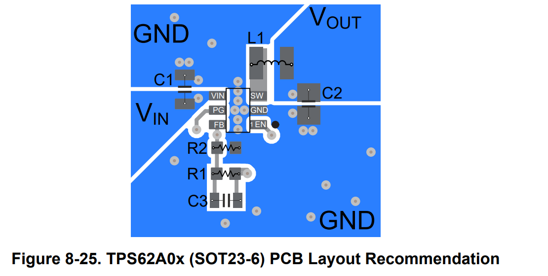
What about layout? Can you just put things wherever for this board like you did with the sensor board with little fear of electrical issues? Not really...the Buck Converter is a switching supply and one that moves a lot of current and makes a lot of electrical noise as well so we need to be a bit more mindful of how we lay things out. Section 8.4 of the data sheet has some pro-tips about laying out the board and then Figure 8-25 (shown below here) is a recommended layout of the board.
Board outline
Open up the PCB layout file (.kicad_pcb, and draw a board outline that is 1000 mils wide by 1200 mils high on the Edge.Cuts layer.
Ratsnest to layout
Import the ratsnest from the schematic and start to lay things out. From the datasheet, the key takeaways for you are:
- Big, short traces on any route carrying a lot of current. The inductor and capacitors we have low series resistances, it would be a shame to throw that characteristic away by putting long nasty high-resistance PCB traces in your circuit introducing lots of parasitics.
- Keep components close by the IC and each other
- Try to electrically isolate the SW terminal (that's the end of the inductor that is going to be kicking all over the place with weird voltages when getting switched).
- Keep the feedback path away from the SW terminal if possible (route around it/try not to go under it).
One thing that would be nice to experiment here is with non-standard traces. You can see in their recommended layout they're clearly doing some nice beefy pours to make sure all the copper is getting used. While big, thick standard traces are definitely good, you may also want to try to emulate these pours. You've done one pour so far, a ground pour on the back side, but now you can get some practice doing some smaller ones.
After positioning your parts in a way that you think will work well, do a small pour on the front copper. When you click, attach it to the net of interest (for example the VOUT net that connects to the output side of the inductor) and set the pad connection to be "Solid" for this pour rather than "Thermal Reliefs" (doing so will allow the pour to connect all the way to the pad. Actually lay out a nice polygon around where you want to connect.
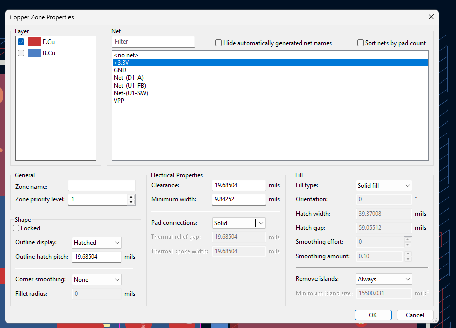
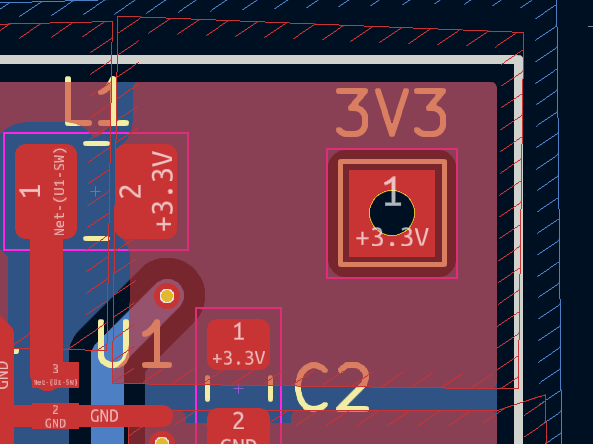
When done, run your pour (the "b" key) and you should have something like this:
Connector
Your connector should be placed in the center of one of the short sides of the PCB, with the outline (on the yellow F.Silkscreen layer) coincident with the edge of the board.
DRC
As always, run and pass your DRC.
Try your best on this layout. Our buck converter and its needs are not too demanding in my experimentation, but who knows, you students always figure out interesting ways to break things so I'm excited to see how your designs turn out.
Submitting your design
Once you are satisfied with your pcb, submit to git. (as a reminder, see the instructions from ex02/sensorboard_schematic for more details about how to set this up)