Sensor board schematic capture
Please Log In for full access to the web site.
Note that this link will take you to an external site (https://shimmer.mit.edu) to authenticate, and then you will be redirected back to this page.
Learning Objectives
One of our goals in this class is to give students the confidence to go beyond the breakout board, meaning that when designing a system, you can fully partake in the rich ecosystem of parts that are out there, and not limited to the <1% of parts that are available as fully formed boards on Adafruit, Sparkfun, etc. A second, related, goal is to teach students how to design, lay out, assemble, and test your own printed-circuit boards (PCBs). Making your own boards enables you to create custom systems that do exactly what you want, nothing more and nothing less. It's super powerful.
Let's get going.
In this exercise, you'll create a schematic for a custom sensor board in an electrical design tool called KiCad. If you want to be extra cool, note that it is pronounced "key-cad". It'll let us capture our design as a schematic, which we'll later turn into a printed circuit board (PCB) through a process called layout. Here, you'll do a little circuit design, and hunt for information in datasheets.
You'll need a working copy of KiCad for this lab. The instructions for getting it are here, along with the rest of the course software.
Why are we doing this?
We can get various breakout boards from vendors, like the BH1750 board that we used in lab01. So why make our own? Four reasons:
-
When we make our own we have complete control over what's on the board. For example, many breakout boards will include a 3V3 regulator on the board. But if we don't want that, we can get rid of that -- fewer components, less cost, less power consumption.
-
We can go beyond the breakout. Breakout boards represent well less than 1% of the components that are out there. Now you can design your team project using almost any part that you can buy on Digikey. That allows for a better design.
-
Teaching. Many of the concepts involved in developing a PCB schematic and layout build on what you learned in 6.200 and related classes. It's a reinforcement exercise.
-
And, finally, being able to create your own PCBs, even simple ones, opens up new vistas. It's a great skill to have, for work or hobby.
The PCB timeline
If you take a look at the calendar you'll see we have a fairly elaborate calendar for the PCB design, which for each board will have 5 steps.
We'll have several things due not on pset due dates, and you'll need to keep track of all this.
Here's how it will go for the sensor board:
- This week we design and draw the schematic.
- Once this is due on Monday, we'll assign every student to peer review 3 other student schematic designs. Those peer reviews are due Thursday.
- Once you get receive your peer reviews, you update your schematic, and then do your layout, due the following Monday.
- Again, everyone will do 3 peer reviews of layouts, due that Thursday.
- Then everyone has a few days to revise their layout. The board files are due for fabrication the following Monday.
So several deadlines of less a few days. We'll work to remind you, but it's up to each student to stay on top of this.
Let's GIT started
We're going to use Git to upload, share, and peer review our PCBs. KiCad is actually pretty compatible with Git at least as far as it coming to archiving and version-controlling your designs (a schematic file is just thousands of lines of markup language...same case with a PCB)1
By now you've hopefully joined the 6-900-S26 organization on github.mit.eduand set up Git on your laptop.
The process for working with Git and KiCad will be the same for each PCB project.
-
We will add you to our course github organization
6-900-S26on github.mit.edu as long as you have a github.mit.edu account. If you don't have an account, we can't make a repo for you, so do that ASAP! -
We will make a repo for you within that organization.
-
Open a terminal. Navigate to the directory (using
cd) where you would like to store your PCB project. For example, that might be a directory named6.900\psetsin your home directory.- Windows users using WSL: Use your
cdwincommand that you created when setting up Git to navigate to your Windows folders. Since KiCad only has access to your Windows folders, you'll want to clone there.
- Windows users using WSL: Use your
-
Clone your repo. In your terminal, run the following command:
git clone git@github.mit.edu:6-900-S26/sensorboard-None.git
The result should be a directory named sensorboard-None.
If you have issues, reach out on Piazza. But if all works well, you're ready to start your design.
Circuit Schematics
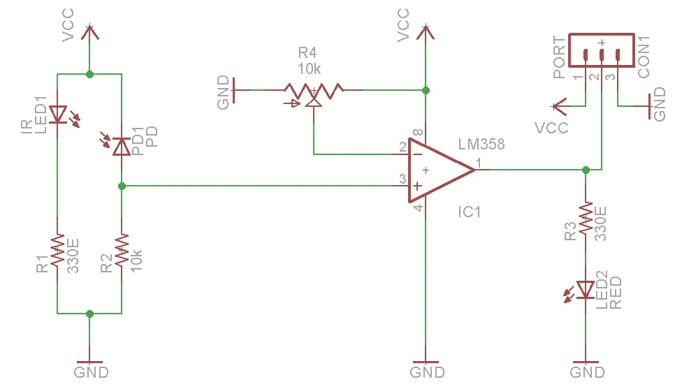
The first step of designing a PCB is drawing a schematic, which depicts all of the components and how they are connected. This process is called schematic capture. Schematics are how electrical engineers represent circuits logically, and let us do circuit design without having to think about where exactly the physical components will live in real life. They look something like this:
KiCad has it's own set of tools that'll help us make sure that the circuit our schematic represents actually works. Schematics are also used by circuit simulators like LTSpice that toss in physical models of each component, and simulate the circuit over time. If you do it right, this helps verify that the circuit you eventually fabricate will perform as expected.
If you haven't used KiCad before or if you want a refresher, we recommend the following tutorials on schematic capture:
Specifications & Design
For our sensor board, we've chosen to use the following sensor:
This sensor is a 3-axis accelerometer, meaning it measures acceleration in x-, y-, and z-directions. Pretty cool. Such a part can be useful for your project, for example to detect if your system is oriented correctly, has fallen over, gotten hit with a baseball bat, that sort of thing.
The sensor communicates with a microcontroller via I2C protocol. It operates and communicates using 3.3V voltage levels.
Thus, our sensor board will include connections for power (3.3V and GND) and I2C communications (SDA and SCL lines).
The sensor also has the ability to send an interrupt, meaning it can drive a line high (or low) based on a particular event happening. We'll want to have a connection for that as well.
What else do we need to specify?
In designing this subsystem, like many others in this class, we need to think through the interactions with other subsystems, as well as test and verification (and thus debugging!). For this first design, we'll basically tell you what you need to include and why. For the next design you're more on your own!
- Connectors: how are we going to get the electrical signals from this board to the others? We'll need cables to do this - but there's an incredibly large selection of wires and connectors to build our cables from. Here we'll use Amphenol's Quickie connectors, with some ribbon cable in-between them. Why? These use something called "insulation displacement connectors" (IDC), which make for cables that are really straightforward to make. And because we don't have any crazy specs in terms of voltage, current, or frequency, this is a fine choice.
In fact, you'll notice that there is already a housing for an IDC connector on our 6.900 mainboard, see here:
So we will want the connector on our sensor board to be designed accordingly so that the correct pins line up on each board.
-
Debugging: we all hope our HW/SW works the first time - but it won't! So you need to make debugging easier. On the hardware side, that means:
- Making sure all important pins on the chips are "brought out" so they can be probed or soldered to.
- Including what are known as test points on key signal paths. Test points allow us to probe the circuit to verify it is working correctly. For this board, think about what signals would be useful to be able to test if the board does not work right away.
- Including status LEDs. It's annoying if you have to hook your system up to an oscilloscope or computer to know if it's on, or working. So we add status LEDs that help us know at-a-glance what's going on.
-
Testing & verification: related to debugging is testing. How do we know if our sensors work? We need to set up tests, same as the "unit tests" in software engineering. For this subsystem, that means testing across acceleration levels and directions. Not easy! We'll return to this later.
Schematic Design on Paper
Before drawing the schematic in KiCad, we will first sketch things out on paper.
IC manufacturers will often provide reference or typical application designs in the datasheets. These show an example design that covers most of the use cases of their specific part - they do this to make your job as a designer easy, so you'll use their parts! For now, we're going to follow their lead, and use their reference designs for our sensor. We'll find that design on Figure 19 of the datasheet.
It's good to work to understand why different components are on the schematic, because sometimes we don't need them, or we need to make changes.
-
C1 and C2 are decoupling capacitors on the power rail. Most ICs have one or two decoupling caps. Nothing to change here.
-
R3 and R4 are the I2C pull-up resistors. We'll need those, because I2C needs one set of pull-ups to work. But what value to use? Check out the notes. It suggests 4k7 (aka 4.7 kOhms), which is a pretty typical value.
- R1 and R2 are listed as not being needed "if the interrupt output driver type is configured for push-pull operation (default)." We are using push-pull, so don't actually need R1 and R2.
- In fact, we are only going to use INT1 for our interrupt line, so we want to ignore pin 6 (INT2/EXT_TRIG_BOOT_OUT), aka leave it unconnected to anything (floating).
What about Pins 3 and 7?
If you scroll up to Table 3 on page 4 of the datsheet, you'll see that Pin 3 is the SA0/SPI_MOSI pin, and the description states that it depends on whether INTF_SEL is set to VDD or GND. Your schematic should show that pin set to GND, consistent with the Pin 9 description in that table to select the I2C interface mode.
So now we know that pin 3 sets SA0, or the "least significant bit of the device I2C secondary address". Every device on the I2C bus has an address, and some ICs let you choose multiple addresses, so that, for example, you can have two IMUs in the same system. Tying this pin to GND or VDD will set that part of the address to 0 or 1. You can choose either, but we recommend tying to GND.
According to Table 3, we find that Pin 7 is the SPI_CS_B/WAKE_UP pin. Again, like Pin 3 it has multiple functions. When BT_MODE = GND (aka pin 2 connected to GND, as we have), Pin 7 is the pin that allows the accelerometer to exit the low-power Hibernation mode. We won't use Hibernation mode in our simple board here, but you will probably want to use it if you use an IMU in your project. So for now, we can tie pin 7 to GND.
Adding a few components for debugging
-
Next, mark the signals that you think will need test points. A simple rule of thumb for us: put test points on each separate signal, aka 3.3V power, ground, SDL, SCA, INT1.
-
Next, we need to add in a status LED. We recommend a status LED on the 3.3V power line so the board lights up when "ON". The LED will need a series resistor connected between the LED's anode and the signal being measured (in this case, 3.3V). This so-called current-limiting resistor (details here) needs to be of the right value so that the right amount of current goes through the LED: too much current and the LED will burn out, and it will consume too much power; too little current and the LED will not turn on or will be really dim. The amount of current depends on the LED. You have a choice of four colors, all from the same part family:
- Red: HSMS-C170
- Yellow: HSMY-C170
- Green: HSMG-C170
- Orange: HSMD-C170
The LEDs' datasheet provides the typical (forward) voltage needed to achieve the 20 mA they use as their standard brightness (see Table 5). That's actually much brighter than we need, and will burn alot of power. We'll instead want a resistor sized to give around 5 mA of current thru the LED. A bit dimmer, but not as wasteful in terms of power. You can assume the same forward voltage even at the lower current. Pick your color, and calculate your resistance given our 3.3V supply voltage.
We don't ask you to hand in the paper schematic, but you'll need it to keep yourself from getting confused as you're putting things into KiCad. We're teaching you both design intuition and a new tool here, and your paper schematic is the bridge between the two - it's your map and anchor. Put some care into it. Once it's complete, let's capture it in KiCad.
Schematic Capture
Fire up KiCad. You should see a window open up. From this main KiCad window, you can make a new project by clicking File -> New Project.
Navigate to the folder containing your repo, such as sensorboard-None.
In the dialog box, type in a name for the File name. sensorboard is not a bad choice.
Very important. Unselect the Create a new folder for the project checkbox, as shown below:
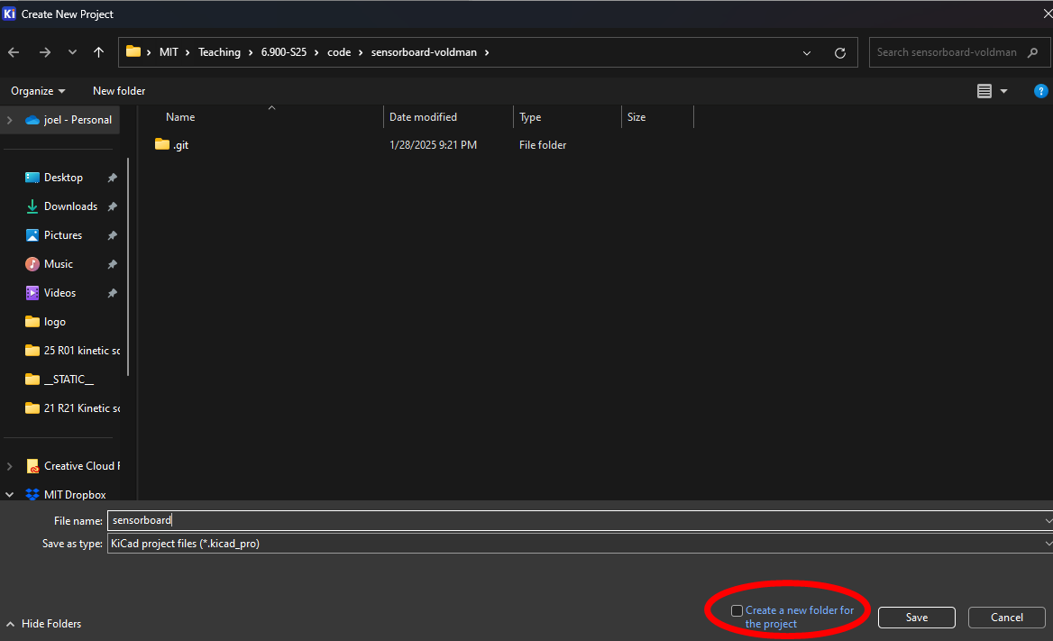
Hit return. KiCad will give you a warning about the selected folder not being empty. It's totally fine. Hit Yes.
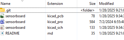
If you do this correctly, you'll have the following project directory:
Next, you'll want to put this KiCad-specific .gitignore lines in your repo's main directory. This will tell Git to not upload KiCad's auto-generated backup files and cache files.
Once you have made a new blank project, the main KiCad window will show 2 blank files in the project directory, a .kicad_pcb file and a .kicad_sch file.
Open the schematic file by clicking on the schematic editor icon.
Placing Components
The first step is placing all the components our circuit needs into the schematic.
Let's add our passive components (resistors, capacitors, LEDs) first. To add a part (or symbol) to our schematic, press the letter A on your keyboard or click on the Add Symbol icon on the right of the schematic editor window.

In the searchbox type in R_US or R (R_US is the American resistor symbol while R is European style symbol) and select the resistor. The symbol will be attached to your mouse cursor and can be placed anywhere on your schematic by just clicking.
If you want to rotate your resistor, select it and press R on your keyboard.

To add more resistors, we can repeat the above steps, or select the previous resistor and copy-paste.
We should probably specify the value of the resistors. To do so, we right click the symbol and open the Properties dialog. Change the text in the Value field of the Symbol Properties dialog box that pops up.
Once you have added and given a value to all of your resistors, add your capacitors and LEDs in the same way. (Make sure to specify each capacitance or color)
Finally, add the Test points. Search for "testpoint" and choose one with only 1 connection.
Add the IC and connector
FXLS8974
Once we have our passive components in place, let's add our Integrated Circuit (IC). As you know, this design requires a FXLS8974 sensor.
If you search for this part in KiCad, though, you'll find it doesn't exist. This IC is not available in KiCad's default part library. To obtain its symbol and footprint, we can download them from an online service.
- Find the exact part on an online electronics component distributor, such as DigiKey or Mouser.
-
Scroll down to the section where the EDA/CAD or ECAD model is listed.
-
Create an account with the library service, if necessary, and download the KiCad-specific library files.
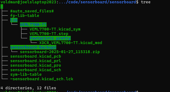
Once you get your hand on the library files, we need to put them into a project specific library folder.
-
In your project's folder, create a new folder called
libin the same location as the.kicad_pcband.kicad_schfiles. -
Inside the
libfolder, create a new folder calledFXLS8974. This is where the sensor's.kicad_symand.step(if you have a 3D model) files will go. -
Within the
FXLS8974folder, move the.kicad_symfile and the folder.prettyfolder.
.kicad_mod file with no pretty directory. If so, just create a pretty directory and move the .kicad_mod file inside it.After all that, your directory structure should look something like this:
The last step is to tell KiCad to look in these folders for our part. Find and open the main KiCad project window:
On the top, open Preferences then Manage Symbol Libraries...
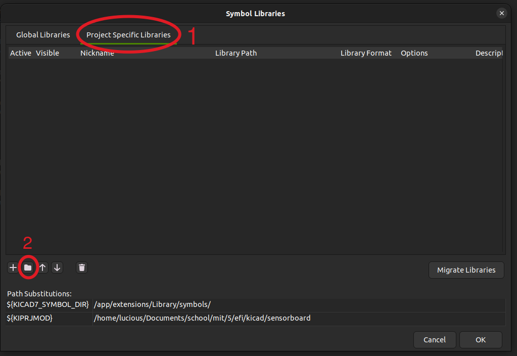
- Click the
Project Specific Librariestab on top (NOT Global Libraries) - Click on the icon of the folder towards the bottom
- Navigate to the part's
.kicad_symfile and select it. Close the dialog box.
If all goes well, you will have added the part's symbol to your project. To add the part's footprint, let's return to the main project window. Once again on the top open Preferences but this time click Manage Footprint Libraries. Repeat the same steps as above (Project Specific Libraries). One difference is that for footprints, KiCad wants a folder that ends in .pretty as opposed to the symbol's .kicad_sym file. Since we spent time organizing the part's library folders, it should be in there.
Now we can finally search for the FXLS8974 and add it to our schematic.
Connector
Now we need to repeat for the 2x3 connector. We are using the Amphenol 75869-131LF. Find, download, and add the part symbol, footprint, and, ideally, 3D Model.
Making connections
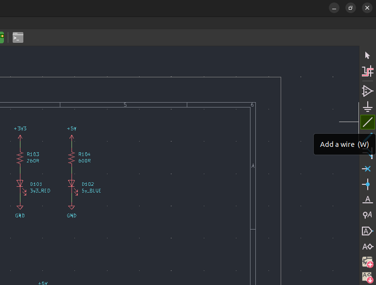
At this point, your schematic should contain a bunch of randomly arranged, unconnected parts. Click the wire tool in the right-side toolbar of your editor, and wire the parts together. This connects them electrically.
You'll also want to arrange your parts so that you don't end up with a ratsnest once everything's connected. You can rotate your parts by hitting the R key with the part selected, and you can mirror the part with the X and Y keys - which one you press determines the axis it's mirrored on.
As you start to draw more than a few wires, eventually your wires will cross and eventually your design will get messy. See the next section below about how to make the design neater via use of Nets. In particular, you may find it useful to have Power and Ground ports in your design, which are again accessible from the right-side toolbar.
Wiring up the connector
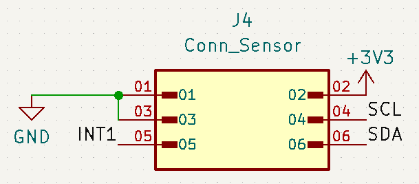
The 2x3 pin connector is intended to connect power and signals to the mainboard. Thus, the particular pins on that connector must correspond exactly to the pins on the mainboard, which we provide below:
Adding Nets / Net Labels
Thus far we haven't had a ton of connections between components, and there haven't been that many components to connect to. That goes away for larger designs, which will turn into a ratsnest of chaos if we only connect things with wires. We'll need some notation to help us keep our schematics tidy and legible. The electrical engineers of yore decided that the best way to do this was by putting a label next to the wire to label the signal - and when we want to use this signal elsewhere, we just put the same label next to that wire, making them electrically connected. This means that everything with the same name is electrically connected.
KiCad (along with most electrical design tools) implements this feature as something called a net, which is just that named wire. We assign wires to nets by throwing a net label on the wire, and any two wires that have the same net label attached to them will be electrically connected. For this to work, the names must match exactly, but we get to pick the names. And as long as we name our nets things that make sense, we can make our schematic make sense to whoever's reading it. Just like variables in code.
Here's an example:
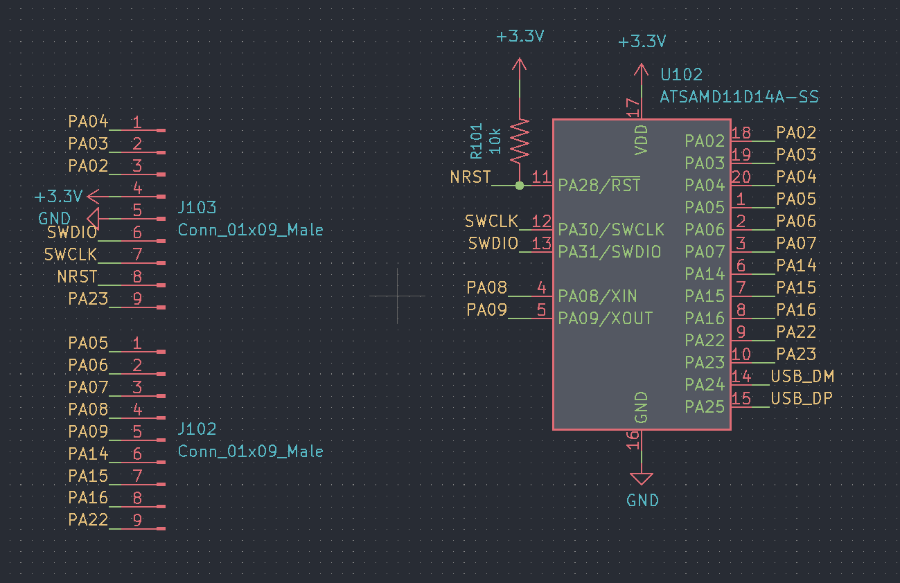
If you notice, we're using net labels for signals like NRST, USB_DM, PA05, and so on.
For the purposes of this class, we would like you to use Net Labels to clarify your schematics. This will make your schematics easier to design and review. An additional benefit to labeling your nets is that it makes the PCB layout stage less confusing. KiCad will present the net names to you during PCB layout. If a net has no label, KiCad will give the net a confusing name which you will have to decipher. Label yo Nets!
The one time we don't want you to label nets is if the pin connects directly to a power or ground net. In those cases you want to add a power port by clicking on the following (or hitting P):
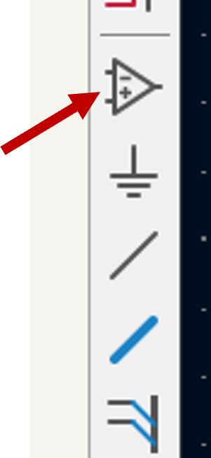
Even though it looks like a ground symbol, it will also allow you to put in power symbols. In the dialog box, you can search for "+3V3" or GND" or lots of other options. Once you've added a power symbol, that will also label those nodes as power or ground nets (so you don't need to add explicit net labels).
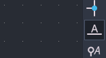
To add a net label, click the Add Label tool on the right hand side of the schematic editor (or press L on your keyboard).
You will be prompted to give the net a name. Give the net a name and then click okay. Your label should look like this:

You can place your net label on an existing net to assign the name to that net. You can also just place the label on your schematic and attach a wire to in as if it were a one-terminal component. Here is an example of the different ways net lables can be used:
No Connect
Remember that pin 6, which we're not connecting to anything? If we actually leave it unconnected, KiCAD will get upset because it thinks you are forgetting to make a connection. So we need to explicitly tell KiCAD that we intend to not connect anything to that pin.
To do that, add a "No Connect" Flag to pin 6 via the "Place No Connect" (Q) command.
Make it pro
Schematics are an electrically accurate, logical representation of the circuit you're going to build. There are two audiences for the schematic -- the layout editor and other humans. The layout editor doesn't care what the schematic looks like, but other humans sure do. Because you're going to need to get your schematic reviewed by other students, and just like code, you want it to be easy to review.
So, here are some good tips for the schematic, beyond getting it functionally correct:
-
Give yourself enough space so that components and their text don't overlap. You can rotate the components, move their associated designator and label, etc. to make things easy to read.
-
Align related components vertically and horizontally.
-
Rename the 'labels" to make more sense. Instead of connector "J1" with name "02x02_Odd_Even", doesn't something like "I2C" or "Power" make alot more sense?
Assigning footprints
To reduce the physical size of our boards, we'll be using surface mount (SMD) components when possible. SMD components are mounted directly to the face of the board rather than requiring a through-hole. Surface mount parts come in a range of standard packages and sizes. For our resistors, capacitors, and LEDs we're going to standardize things by always using 0805 parts. 0805 refers to the dimensions of the package, in this case 0.08" by 0.05" (or, 2 mm by 1.2 mm, for those in societies without a manned lunar program). This choice is a bit arbitrary, but 0805 parts are common, small enough to create compact boards, and large enough to put together by hand.
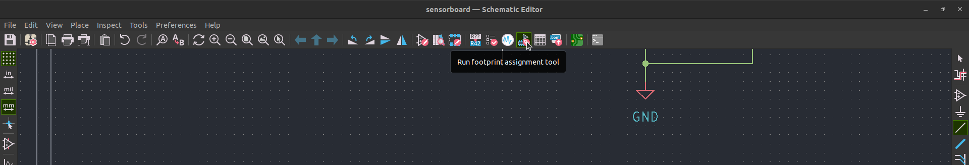
To assign footprints to our parts, click on the Assign Footprints... / Run footprint assignment tool button on the topside toolbar.
The list on the left contains all of the currently accessible footprint libraries. The list on the right shows each footprint within the selected library. The list in the middle are all of the parts present in your design.
To assign the 0805 footprint to the resistor, lets do the following:
- Find the
Resistor_SMDlibrary on the left. - Find the
R_0805footprint on the right. There will be two. (one has larger connection pads that are easier to solder by hand; choose this one :-) ) - Once it's been selected, copy it into your clipboard using your OS-specific clipboard keyboard shortcuts.
- Select one of the resistors present in your design (middle list) and paste the footprint on your part. Rinse and repeat for the other resistors in your design. (Protip: select multiple resistors (click on the first, hold shift and click on the last) in your design and paste them all at once)
Great. Now assign the capacitors and LEDs with their respective 0805 footprints.
Your FXLS8974 has a set of different possible footprint. Choose the "-M" variety, which is the maximum sized one that is easiest to hand-solder.
And then repeat for the connector.
The last footprint to assign is our test points. For ease of connecting to the test points, we suggest you assign the TestPoint:TestPoint_THTPad_2.0x2.0mm_Drill1.0mm footprint.
After you have assigned the footprints, Apply, Save Schematic, & Continue and press OK.
Final Schematic Requirements
Before moving on, your schematic should meet the following requirements. Your schematic should have:
- One 2x3 six-pin connector with pins connected as in the figure above
- A LED (in an 0805 package) indicating when the board is connected to power.
- Test points on SDL, SCL, 3.3V, and ground nets for debugging. The test points can be placed anywhere on those nets.
- Appropriately named nets for SDA, SCL, GND, and 3.3V.
- The FXLS8974 should be wired to 3.3V, GND, SDA, and SCL according to its component datasheet.
- Very likely 3 resistors and 2 capacitors.
ERC
Every time you make a schematic you'll want to run the Electrical Rule Check (ERC), which is a set of automated checks it does to make sure your design looks okay. You can run from (Inspect / Electrical Rules Checker / Run ERC). An ERC button is also in the top toolbar.
You'll probably get some errors that say "Input power pin not driven by any Output Power pins". These you can safely Ignore by right-clicking and selecting "Exclude this violation".
Send it on up
Now let's push all these files up to the github.mit.edu repo. It's actually good practice to go thru these steps after you make any major change to your design, not just when you are ready to do your final submission. By pushing changes along the way, you ensure you don't lose any work.
We're going to be using a stripped down set of git commands here, but if you want to learn a bit more about what's going on, I like the tutorial on the 6.102 website, and there are many others online.
First, you need to stage the new and/or changed files.
git add .
This will add all the files in the folder (and subfolders) to this repository. Next do a commit so this initial add is all included. Something like:
git commit -m 'initial add of files for design'
Always add a useful comment in your commit statement. Don't be that person who writes changed stuff.
git push origin main
If all works well, your files should now be up on github.mit.edu. You can check on this by looking at the repo on your browser.
You can keep updating your project and pushing changes to the repo. We'll use the latest timestamp to assess lateness, so make sure your final push is before the due date!
What's next
Right after the schematic is due, we'll assign 3 people to review your schematic. We'll also assign you to review 3 student's schematics.