Sensor board PCB layout
Please Log In for full access to the web site.
Note that this link will take you to an external site (https://shimmer.mit.edu) to authenticate, and then you will be redirected back to this page.
In ex01 we captured the schematic of a circuit for sensing temperature, relative humidity, and light level. Now, we're going to layout the board, and get it ready for fabrication.
We'll actually fabricate these and give them to you, meaning that any mistakes you make in your boards, you'll have to live with. You're more than welcome to speedrun this layout, but if you do you'll spend hours fixing your PCB once it's back from the factory - assuming it is even fixable at all. So keep an eye for detail and ask us if you've got questions! We want to make sure you'll end up with working boards - and as the bitter, tongue-in-cheek saying goes, half a day in the lab saves fifteen minutes of layout.
Schematic design review & fixes
Before you start the layout, you'll want to:
- Perform your designated schematic design reviews of your peers' design
- Look over the three design reviews of your own schematic
Do a pull to get your design reviews:
- Open a terminal
- Navigate to the directory containing your KiCad project
- In that directory, type:
git pull
If all works, you should have three new *.md files in your directory.
Updating your schematic
Go thru the three reviews. If they find errors or critical style issues, fix them in your KiCad schematic. If there's a note there that is confusing or you don't agree with, please reach out to the staff.
There's no addition design review after your changes. Now we go to the layout!
What's ok?
You did 3 reviews of other students' designs. In fact, you know have their designs on your laptop. Sure, it's fine (and good) to be inspired by them, and feel free to adapt your schematic accordingly. But you cannot simply copy your peers' designs. That's not ok.
What's a PCB?
A PCB is a Printed Circuit Board, and fundamentally it’s just a flat piece of material that connects electronic parts together. You’ve likely seen them before, but here’s a couple examples of what they can look like:
Those are called rigid PCBs, and they’re made by taking a flat piece of fiberglass substrate, bonding conductive copper to either side, and then selectively etching away the copper to make connections between the components you want. Components mount to either the surface of the board, or they have leads that go through the board and solder to the hole. It’s basically a fiberglass sandwich, and looks like this if you slice into it:
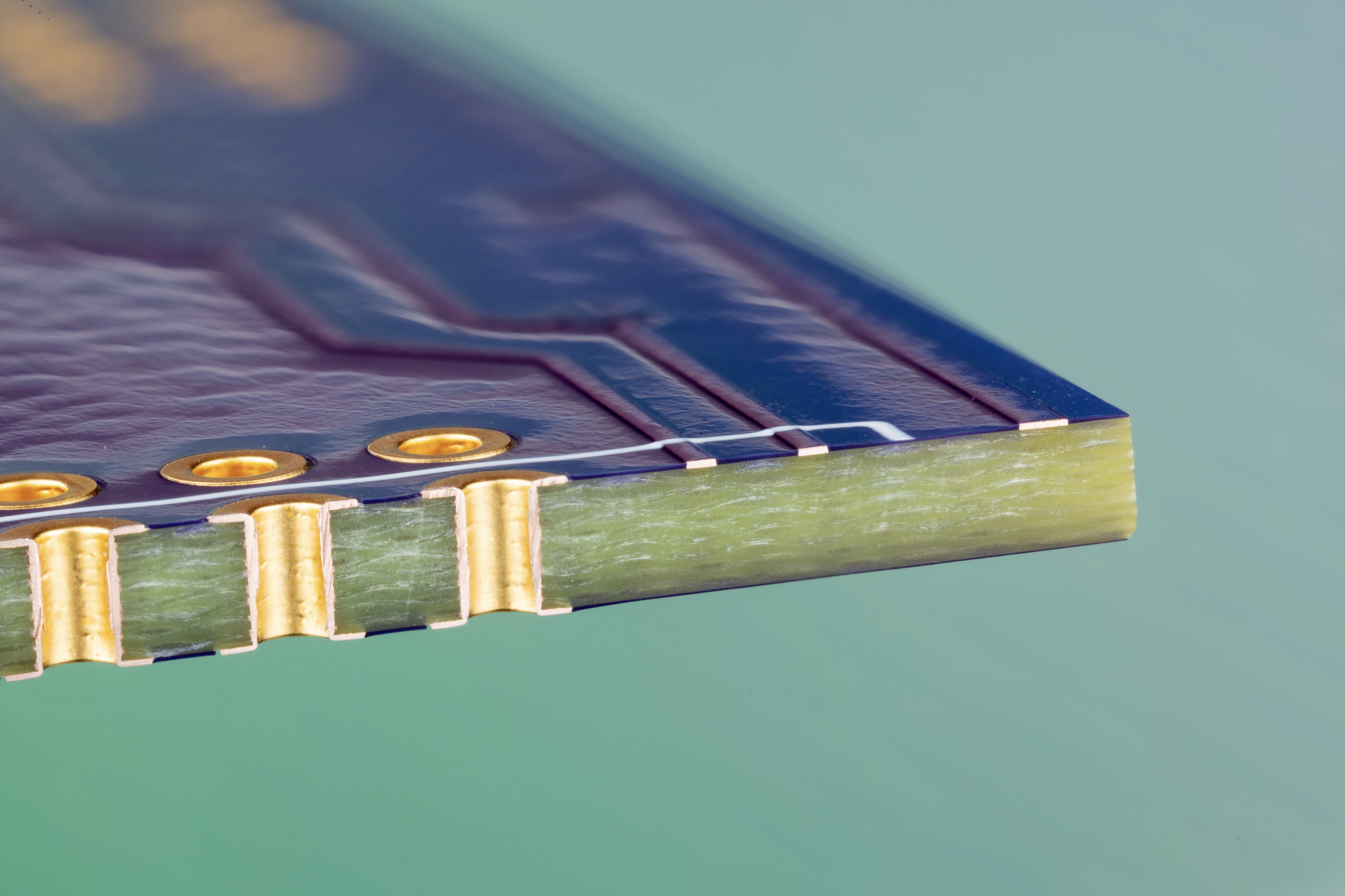
If you'll notice there's a layer of pretty purple that goes over the copper on the top and bottom of the boards. That's called soldermask, and it keeps solder off parts of the board it shouldn't be on. This will make more sense when we assemble boards, but it only exposes the parts of the copper that are necessary to make solder connections, and protects the rest of the copper from oxidizing. On top of this soldermask is the silkscreen, which is the white line on the board above. This is used for marking up the board, which we'll use to label parts, add version numbers, and a few other things. It's applied in the same way that you'd silkscreen a t-shirt, so it gets the name.
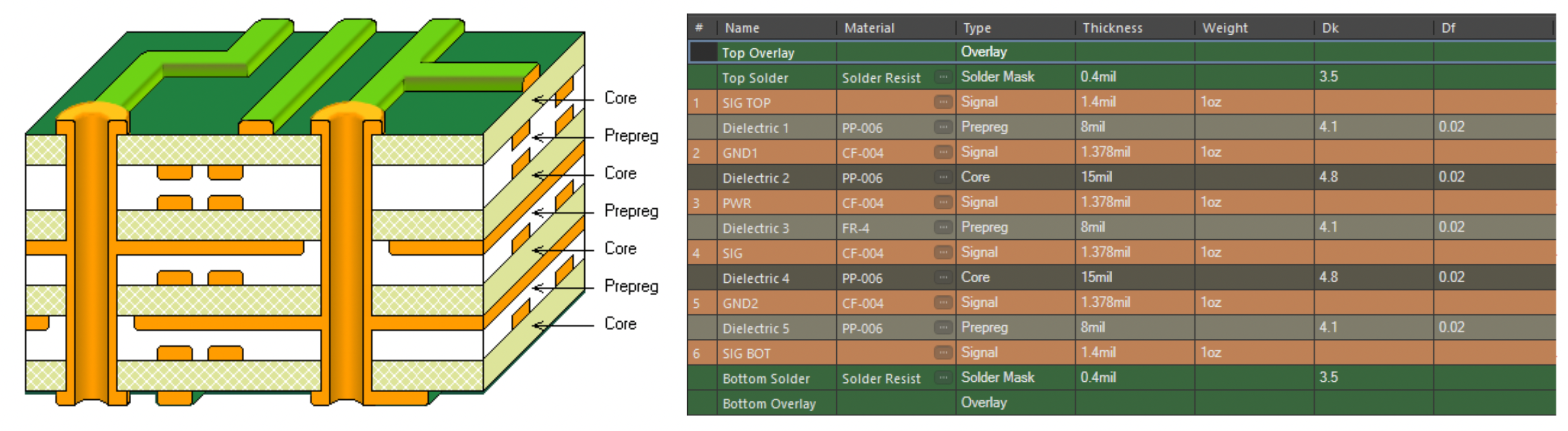
This whole affair is called a rigid PCB, because we're using a rigid, inflexible core, and it's what you'll be designing here. It's the most common type of PCB, but there's plenty of variations. You'll be designing a rigid board with two copper layers in the stackup, hence referred to as a two-layer rigid PCB or just two-layer board. The most common variation on this is a multi-layer board, where we add more layers of copper, separated by insulating fiberglass. Just for clarity, here's what the stackup would look like:
How do we make a PCB?
Making a PCB has a few steps, listed below:
- Circuit Design - where we choose the circuit that will accomplish the desired function within the provided specification.
- Schematic Capture - where we capture our circuit into a digital representation in our CAD tool.
- Board Layout
- Placement - where we choose the location of the parts on the board.
- Routing - where we actually draw the copper wires between components (called traces) and electrically connect them.
- Design Rule Checks (DRC) - where we run some automated checks on the design to look for simple mistakes - unconnected parts, short circuits and the like.
- Gerber Generation - where we make the design files required by the fab, which are called gerbers.
- Gerber Validation - where we double-check our gerbers to make sure they contain the parts they should.
- Fabrication - where we send our gerbers out to be fabricated by a fab house or fab. We'll be doing this part for ya.
We finished the circuit design and schematic capture in ex01, and now we'll run through the rest of the process. There's a lot on this list, but our design is small enough that we'll be able to get our bearings pretty quick.
Board Setup
When in PCB mode, if you go to the Board Setup option in the upper left (next to the save icon), under Design Rules there is a field called Net Classes. In there, if you made net classes in your schematic you can specify PCB-specific attributes to those net classes (for example, making the power/ground connections much larger (maybe twice the width) would be a good idea). Note when creating and grouping Net Classes in the schematic view, this option is not available (since that only handles schematic-specific attributes of net classes like line width/color)....in the PCB you can specify physical attributes. With this done, when you then route pins, you can rest assured that Kicad will automatically set the right width for you and you don't have to worry about forgetting!
Stackup and Design Rules
Board Size
I know it's not on the list, but before we jump into layout we'll want to set the dimensions of the PCB we're going to make. To make things easier on the fab we're going to require all of your designs to be 2" x 1.5".
To make things easier for you, we have already made a template pcb with the correct dimensions and design rules. You may download it here. To use it in your project, replace the premade .kicad_pcb in your project directory with ours. You will have to rename the new file with the original file's name. You will also have to import the settings from this example project file. Download this file, and replace your projects original .kicad_pro file with it.
Placement
Getting Parts on the Board
Open up the PCB Editor from the KiCad main panel. Now that our board's the right size, we'll jump into layout by putting parts on our board. But there's no parts on the board right now! Let's fix that by hitting Tools -> Update PCB from Schematic. A little dialogue should pop up, listing all the changes to be brought into your circuit board.
Hit Update PCB. Close the box, and go back to your layout.
Now, all your parts are floating off in space, and its your job to logically place them on the board. We want our parts to be arranged such that components that connect to each other should be physically close to each other. This makes our wires short, which helps with signal integrity, and our parts tightly packed, which helps us not pay the board fab for more board space than we need.
You'll do this by moving and rotating parts as you move them onto the board. The little grey wires are called airwires, and they show what components need to be connected to each other. As you move the part, they'll move with it. And once you draw the connection with a copper trace the airwire will go away.
A good way to start is to move components that are electrically close on the schematic to be physically close on the PCB. So toggle back and forth between the schematic and the PCB. Place the LED and it's current-limiting resistor close to each other and to the 3.3V pin on the power connector. Place the SH40 bypass capacitors near the SHT40 IC, and so on. Then, once parts are grouped like this, do final placement, with some tips below.
Hotkeys
A decent list of hotkeys is provided here. 1
A few other things
As you're trying to figure out the optimal placement for everything, there's a few things we're going to ask you to think about:
-
Bypass Capacitors: For reasons that we've relegated to footnotes2, we put capacitors near the power pin on every chip. Our sensors are physically rather small, so they've only got one power pin, so we'll throw one or two bypass caps on those chips. If we had something larger (like a microcontroller) that had multiple power pins, we'd bypass each of those. But regardless of the number of bypass caps we'll need, make sure to put them close to the power pin they're bypassing.
-
Mounting Holes: Later on we'll design a 3D printed enclosure, and we'll need to make sure the board doesn't rattle around inside the case. There's a few ways of keeping your boards retained - plastic clips, 3D-printable tabs, mounting holes, hot glue...the list goes on. As a good start, we'll ask you to throw some mounting holes on your board. You can do this by adding a pad to your board (Place -> Footprint), and selecting a
Mounting Holefootprint. We'll design for a M3 screw. Be logical about the quantity and location of your mounting holes. I'm not saying that I won't be impressed if you draw a wojack on your board out of M3 mounting holes, but that's not quite what we're looking for. -
Connectors: You can put connectors anywhere, but typically they're near the edge of the board. We suggest you do that. Also make sure that pin 1 (i.e. the orientation of the connector) is easily discernible. If you chose the right footprint, it should be marked with a square trace thru-hole instead of a circular one! You can also make a marking on the silkscreen layer.
-
Parts on the Backside: While you can place parts on the backside of the PCB, we strongly advise against it due to potential issues with assembly and mechanical stability. You have plenty of space on this board for all your components on the front side. You have been warned! To flip a selected component on to the other side of your PCB, press
F. You would notice (if you had selected an SMD part) that the color of the pads changed from red to blue and were mirrored. Thru-hole parts will also be mirrored but they will stay yellow. -
Label: It's common to add a label on the silkscreen with what the board is, its version number and when you made it, along with your name and email. The reason for this is so that the end user can contact you if something goes wrong - same reason why you put your name and contact in your source code. Go ahead and add this to the top silkscreen layer by adding text to the F. Silkscreen, and/or B. Silkscreen layer.
-
More Label stuff: On your board there is some text is yellow. If you double-click on it you'll see that it is on layer F.silkscreeen, aka on the front-side silkscreen layer. Great. Those are typically the component designators (R1, U1, etc.). And those will be helpful during assembly. But it will also be helpful for some of the text in light grey (which is on the F.fab layer) to also end up on the silkscreen, for example the labels for the connectors -- so you know that J1 is the power connector (or not!), or that TP3 refers to a particular signal and don't have to look it up each time you want to probe it. To fix that, double-click on the text items that you want to move from F.fab to F.silkscreen and select the F.silkscreen layer in the dialog box. When you're finished, turn off the F.fab layer by clicking on the eye in the righthand layer panel.
-
Designators: The component designators we assigned during schematic capture are now on the board, and they're how we'll identify which part is which. But to make your boards look pretty we'll ask that all the horizontal/vertical text goes in the same direction (ie, all the vertical text is consistently ascending or descending, and similar for the horizontal font). The default font size is okay - we can go smaller but we don't really have a reason to. It'll just make board assembly more annoying.
-
Pin headers: If you have more than one set of pin headers and wish to make your PCB breadboard friendly, make sure the headers align to a 100mil grid.
This will likely take you a while - and that's okay! When I'm doing layout I usually spend about 90% of my time on placement, and only 10% on routing. If you do your placement correctly, routing will be super straightforward! As with anything else in this class, if you are having trouble with this please do not hesitate to ask us for help. :)
Routing
In order to route the board in KiCad, you'll begin by drawing copper traces. You can do this by selecting the Route Tracks tool from the toolbar on the left side of the PCB editor window or by pressing X. For this assignment, we recommend you use 10mil trace width for signals and 30mil width for power. To change the width of the trace, you can pre-select a desired size in the Track Width dropdown located at the top toolbar before starting to route. Alternatively, you can adjust the width on-the-fly by pressing W to cycle through predefined trace widths.
When routing the wider power traces to the ICs, you might find that the trace width is wider than the pad width. If so, you'll want to narrow the width of the trace as it approaches the IC pad.
Adding vias to route signals through the board can be done by pressing V or by selecting the via tool from the left toolbar. We'll stick with the default via size for simplicity, but you can customize individual via properties or modify the default via size in the Design Rules if necessary.
When wiring the board, it's recommended to first connect all signals excluding the ground. Begin with shorter connections before tackling longer ones. As you complete connections, the corresponding airwires will disappear, indicating a successful route. Routing is often an iterative process; you might need to move parts or existing wires to optimize space.
For ground connections, adding a ground plane is beneficial. In KiCad, you can create a ground pour on the bottom layer by selecting Place -> Add Filled Zone. In the Copper Zone properties window, set the Net to GND and the layer to B.Cu to connect it electrically to ground and be on the backside of the board. This ground plane helps reduce electrical noise and simplifies grounding. You can absolutely have other signals be a plane if desired, but we usually reserve it for very commonly needed nets, in particular your positive and negative ends to your power supply. This minimizes routing difficulties as well as ensures you have minimal ohmic losses on your power supply path wherever possible!
Now, select Edit -> Fill All Zones (or press B on the keyboard). You'll see the software fill the entire backside of the board with blue, except in areas where you used vias to create backside traces.
Now, with the ground pour done, you can wire up all your grounds. First, if you zoom into one of your connectors, or your Ground TP, you'll notice there KiCad has placed connections from the GND to the ground plane automatically. Thank you KiCad!
The only other thing that's needed is to wire the GNDs for the components, by starting a wire from a ground pad, then adding a via to the ground pour side. So the grounds will end up looking like little wire stubs + vias. Nice and sweet.
If changes are made to the layout, you'll need to update the ground pour manually by right-clicking on it and selecting Zone -> Fill all Zones (or press B on your keyboard). It's advisable to route most signals on the top layer to maintain large, unbroken areas in the ground plane on the bottom layer.
Design Rule Check (DRC)
After routing, including all ground connections with vias to the ground plane, proceed to the Design Rule Check (DRC). In KiCad, access this by going to Inspect -> Design Rule Checker and run the check to identify and correct any issues. It's default settings can sometimes be a little conservative, so in addition to catching things that'll definitely break your design (traces you forgot to route, or traces that overlap and short out) it'll also catch things that might break your design. We'll leave it to your intuition to figure out which are which, but ask if you'd like us to have a look! Peer will check your work at the end anyway.
Gerber Generation
For Gerber generation, KiCad uses a direct export feature. Navigate to File -> Plot to access the plotting window, where you can select layers to generate Gerbers for and configure other settings. Additionally, generate the drill files by selecting Generate Drill Files in the same window. These files are necessary for manufacturing the PCB.
Ensure to review the generated Gerber files using a Gerber viewer to confirm that all layers are correctly represented. Once satisfied with the design, you could upload the Gerber and drill files to a PCB manufacturer (We will do this for you).
Finally, when you are ready to submit, push your changes to git:
git add .
git commit -m '[useful messsage]'
git push origin main
Footnotes
1Taken from here
2 The traces on your board act as antennas that unintentionally radiate the signal they're carrying out of the trace, into other traces and the environment. Take a bunch of traces on a board transmitting into and out of each other all the time, and you get a bunch of noise. We don't want this noise getting into the power rails of our chip, because power gets routed to pretty much everything inside the chip, so any noise in power is seen in pretty much the entire chip's outputs. Which is bad. And there's another reasons why we'd want bypass capactiors, but I'm out of space in this footnote.