Buck converter board schematic capture
Please Log In for full access to the web site.
Note that this link will take you to an external site (https://shimmer.mit.edu) to authenticate, and then you will be redirected back to this page.
Timeline
We have several PCB-related activites going on this week.
- This week we do peer review of the sensor-board schematic and then do the layout
- This week we also draw the buck converter schematic
Several of these deadlines are only a few days away!
Learning Objectives
In this exercise, you'll create a schematic for a custom buck converter in KiCad. This will give you more experience with PCB design.
The power subsystem
We're eventually going to have two parts of our power subsystem:
- A battery manager that can charge a battery from USB and power the rest of our system off the battery or USB as needed
- A buck converter that will take the raw voltage coming off the USB (~5V) or battery (~3.7V) and output a clean 3.3V with enough current
Here we're doing the buck converter portion of the subsystem. We're designing these bits as separate boards to give you experience with the process and to keep the design of each board relatively simple, but in your project you'll likely want a single board for your power subsystem.
Specification and the TPS62A01
Since we've decided on a buck converter, we have to specify one. There are roughly 25,000+ buck converters available on DigiKey. How do we pick one?
This goes back to our specifications. For your semester project, you're going to have to specify what voltages & currents are needed by your components, what is your power source, size constraints, and so on. That will lead to a set of specifications for your power subsystem and the components on there, including any converters/regulators you want.
Here, we have several specifications:
- Converter type: buck as opposed to LDO.
- No. of outputs: 1. Some converters can make multiple different voltages.
- Input voltage range: from 3.5 V (for a mostly discharged battery) to 5.2 V for USB. Here it's nice to select parts a little outside that range as well, say down to 2.5 V and up to 5.5 V, since those would also be fine. We do need to remember, though, that the buck isn't going to be able to output 3.3 V if the input voltage from the battery is <3.3V (it's not a buck-boost converter).
- Output voltage: Output of 3.3V. Some converters have an adjustable output (you can choose the output voltage using resistors), while others have a fixed output. While we only need 3.3V for our system, it would be nice to choose a part with an adjustable output, since then you can use that part for your project if you require a different voltage.
- Output current: 600 mA output current. Our main power consumer is the ESP32C3. The datasheet specifies that the peak current during WiFi TX is 335 mA. We want some headroom above that, so let's pick 600 mA min (more is always better, though more $$$).
- Package: we want something surface mount (not thru-hole) that we can hand solder. So ideally something with leads that we can see, like a SOT or TSSOP package, rather than a DFN. There's also no need for a part with lots of pins -- it's functionality we're not going to need and it's going to make hand-soldering a nightmare.
- We want something "in stock", "active" product status, and sold by DigiKey itself (so we're going to exclude Marketplace)
If you go to DigiKey and select the "Voltage Regulators - DC DC Switching Regulators" product segment, you'll see a bunch of filters show up. Basically, you want to start filtering based on your specs until you get to a reasonable list of products. Using all the filters listed above, I return 109 results. Then I either filter on "price" (cheap is good), or quantity avail (typically products with more avail are more popular, which means they're probably pretty good).
We've chosen the TPS62A01 from this list. It's adjustable,and it's super cheap, at less than $0.10 in quantitites of 100. But that's not enough: there are two different types of packages: SOT563-6 and the SOT23-6. We choose the bigger one: SOT23-6, because we're hand-soldering. In an application where space is at a premium, you'd choose the smaller package. That gets us to a unique part number: TPS62A01PDDCR
Design the circuit
As opposed to the mostly digital sensor board, this board is power electronics, which are mostly analog, and often 2nd-order issues dictate performance. So we need to be more careful with the design, especially next week when we get to the layout.
Find the TPS62A01 datasheet online. There's lots on there, but we basically want to focus on section 8 (specifically Figure 8-1), which goes thru the design of a "typical" application, which is exactly what we want. You'll see that not only the value of the L and the Cs matter, but their composition and secondary characteristics. Luckily, the datasheet does recommend certain nominal values that work for typical designs such as ours.
Choose C1, C2, C3, and L according to the datasheet.
In addition, you need to choose R1 and R2 to set the output voltage value close to 3.3 V (within +/-2%) using resistor values from the E96 resistor series and with R2 close to but no larger than 100k.
You'll also want to include testpoints and at least one status LED (either on the output side or on both sides). Remember that the status LED will need a current-setting resistor.
Clone your repo
As with the sensor board, we'll use Git and github.mit.edu.
-
We will create a repository for you on github.mit.edu.
-
Open a terminal. Navigate to the directory (using
cd) where you would like to store your PCB project. For example, that might be a directory named6.900\psetsin your home directory.- Windows users using WSL: Use your
cdwincommand that you created when setting up Git to navigate to your Windows folders. Since KiCad only has access to your Windows folders1, you'll want to clone there.
- Windows users using WSL: Use your
-
Clone your repo. In your terminal, run the following command:
git clone git@github.mit.edu:6-900-S26/buckboard-None.git
The result should be a directory named buckboard-None.
If all works well, you're ready to start your design.
Schematic Capture
Fire up KiCad. Start a new project by clicking File -> New Project.
Navigate to the folder containing your repo, such as buckboard-None.
In the dialog box, type in a name for the File name. buckboard is not a bad choice.
Very important. Unselect the Create a new folder for the project checkbox, as shown below:
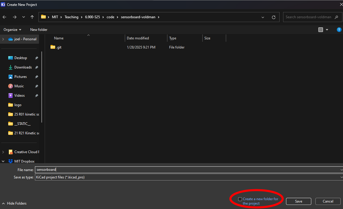
Hit return. KiCad will give you a warning about the selected folder not being empty. It's totally fine. Hit Yes.
Copy over the kicad.gitignore file from your sensorboard repo to this repo so we can re-use it.
Open the schematic file by clicking on the schematic editor icon.
Now add components and wire them up, same as for the sensorboard. Lucky for us, you'll find the TPS62A01PDDC symbol with an already-associated SOT-23-6 footprint in the the default KiCad library, so no need to go to the Internet to find it.
There are two different voltages in this schematic, the 3V3 output, and the input, which can vary in voltage. For the 3V3 output, it's hopefully obvious which power port to use. For the input, you can use VPP, VCC, VBUS, anything like that.
For the connector, because we are going to plug this board into the right-angle header that is currently being taken up by the LDO board, we want the same connector and pin arrangement. Namely, use a Conn_01x03_pin part, with pin assigments of: 1 - Input voltage 2 - 3.3V output voltage 3 - Ground
Assigning footprints
When everything is wired up, assign footprints. For the capacitors, resistor, LED, use 0805 footprints. For the TPS62A01, it will already have a footprint.
The inductor will have a 1008 hand-solder footprint.
For the connector, use Connector_PinSocket_2.54mm:PinSocket_1x03_P2.54mm_Horizontal footprint, which is a right-angle 1x3 thru-hole socket.
ERC
Then run and make sure you pass your ERC.
Final Schematic Requirements
Before moving on, your schematic should meet the following requirements. Your schematic should have:
- One (1) three-pin connectors with the same pin assignments as on the mainboard.
- A LED (in an 0805 footprint) indicating when the board is connected providing output power. You could also have an LED on the input side if you want.
- Test points on input, output, and ground nets for debugging.
- Appropriately named nets for Input, GND, and 3.3V.
- Three (3) caps and an inductor.
- The TPS62A01 symbol and -MFG footprint
- All the correct footprints as noted above.
Send it on up
Now let's push all these files up to the github.mit.edu repo. It's actually good practice to go thru these steps after you make any major change to your design, not just when you are ready to do your final submission. By pushing changes along the way, you ensure you don't lose any work.
git add .
git commit -m 'a useful comment'
git push origin main
If all works well, your files should now be up on github.mit.edu. You can check on this by looking at the repo on your browser.
You can keep updating your project and pushing changes to the repo. We'll use the latest timestamp to assess lateness, so make sure your final push is before the due date!
What's next
Right after the schematic is due, we'll assign 3 people to review your schematic. We'll also assign you to review 3 student's schematics.