MILO sensor board PCB layout
Please Log In for full access to the web site.
Note that this link will take you to an external site (https://shimmer.mit.edu) to authenticate, and then you will be redirected back to this page.
MILO Sensor Board Layout
In ex01 we captured the schematic of a small circuit for sensing temperature, relative humidity, and air quality (VOC/NOx). Now, we're going to layout the board, and get it ready for fabrication.
We'll actually fabricate these and give them to you, meaning that any mistakes you make in your boards, you'll have to live with. You're more than welcome to speedrun this layout, but if you do you'll spend hours fixing your PCB once it's back from the factory - assuming it's fixable. So keep an eye for detail, and ask us if you've got questions! We want to make sure you'll end up with working boards - and as the saying goes, a few hours of bodging saves fifteen minutes of layout.
What's a PCB?
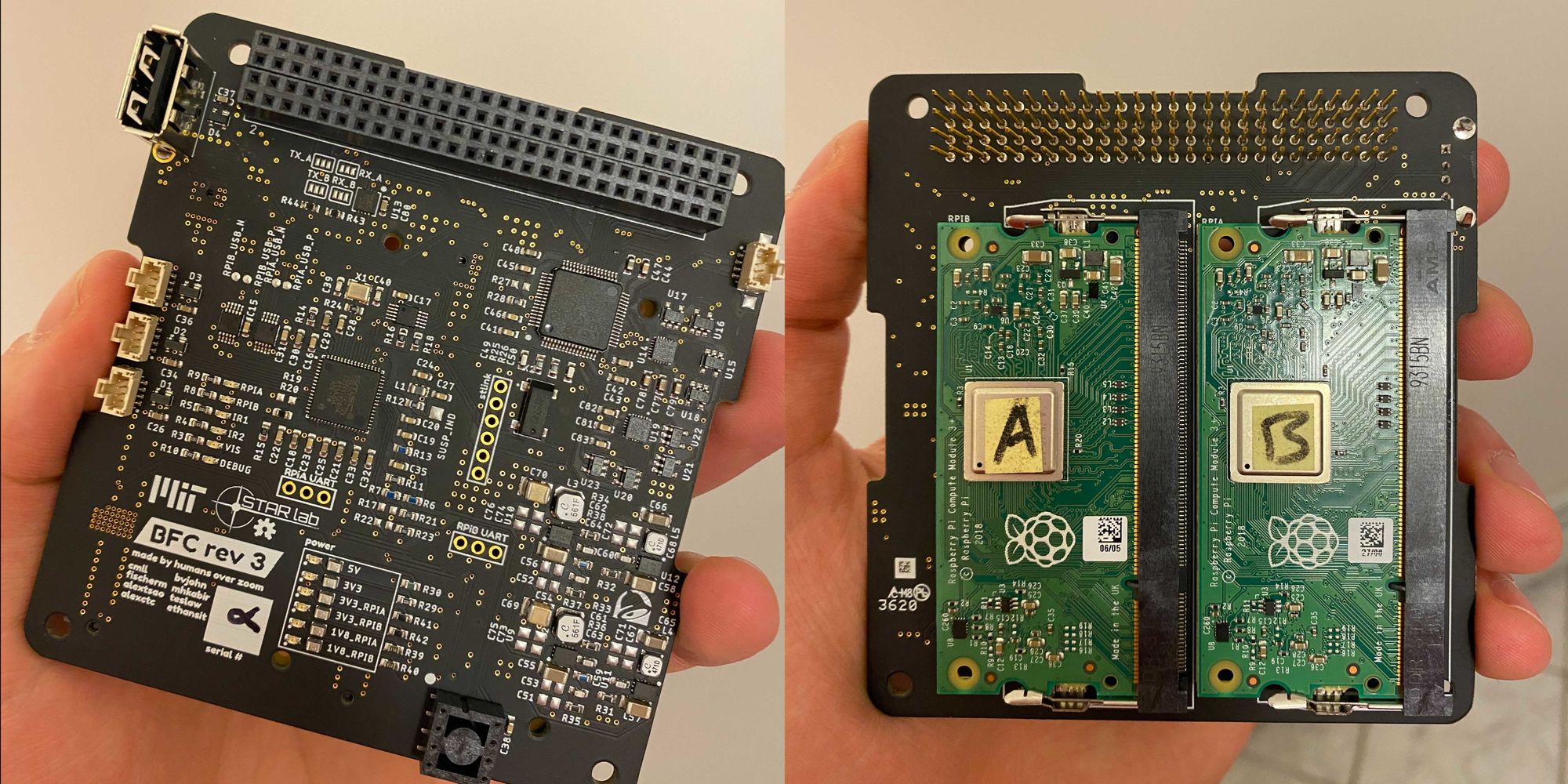
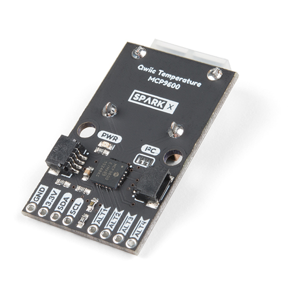
A PCB is a Printed Circuit Board, and fundamentally it’s just a flat piece of material that connects electronic parts together. You’ve likely seen them before, but here’s a couple examples of what they can look like:
Those are called rigid PCBs, and they’re made by taking a flat piece of fiberglass substrate, bonding conductive copper to either side, and then selectively etching away the copper to make connections between the components you want. Components mount to either the surface of the board, or they have leads that go through the board and solder to the hole. It’s basically a fiberglass sandwich, and looks like this if you slice into it: m
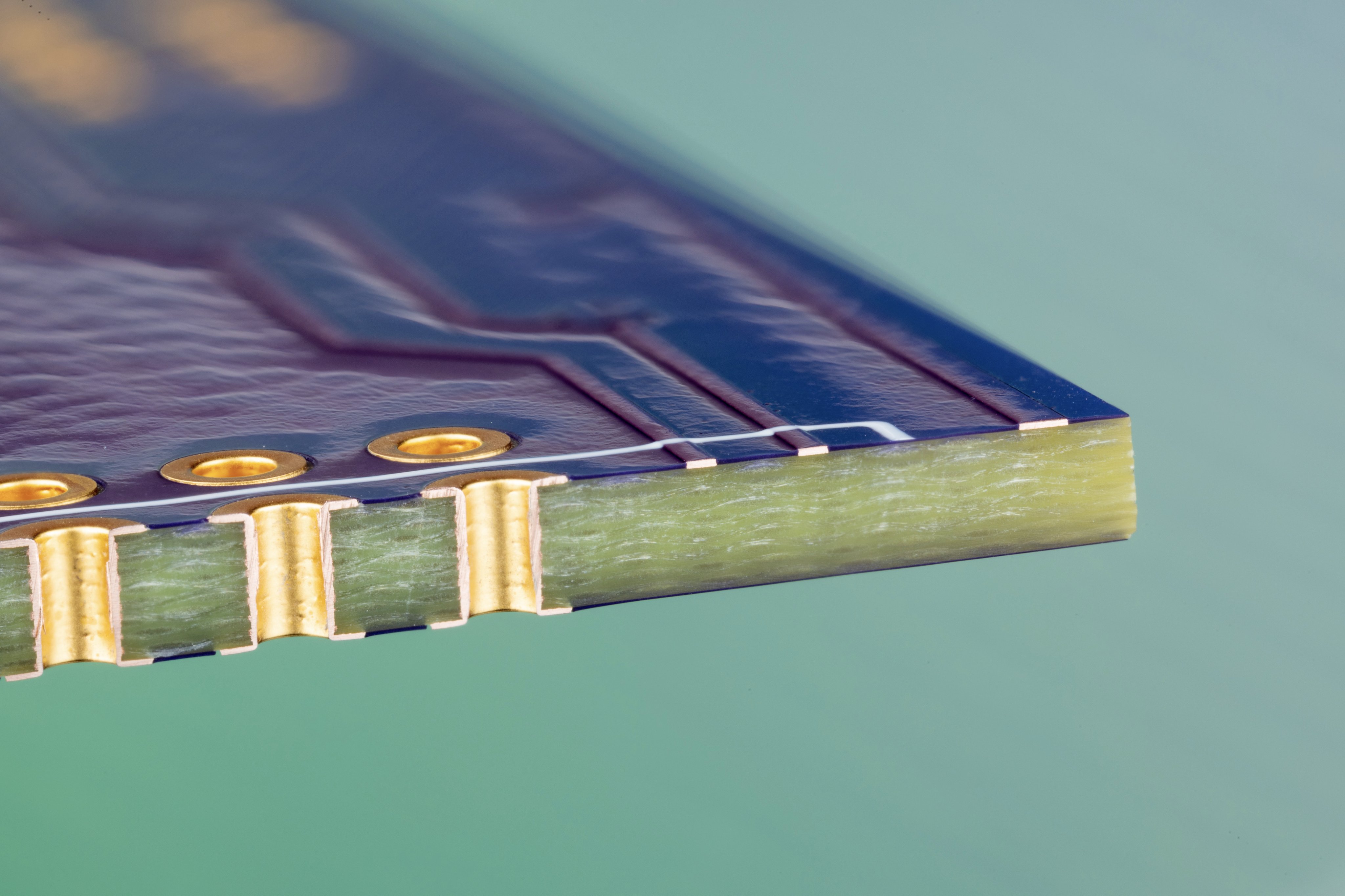
If you'll notice there's a layer of pretty purple that goes over the copper on the top and bottom of the boards. That's called soldermask, and it keeps solder off parts of the board it shouldn't be on. This will make more sense when we assemble boards, but it only exposes the parts of the copper that are necessary to make solder connections, and protects the rest of the copper from oxidizing. On top of this soldermask is the silkscreen, which is the white line on the board above. This is used for marking up the board, which we'll use to label parts, add version numbers, and a few other things. It's applied in the same way that you'd silkscreen a t-shirt, so it gets the name.
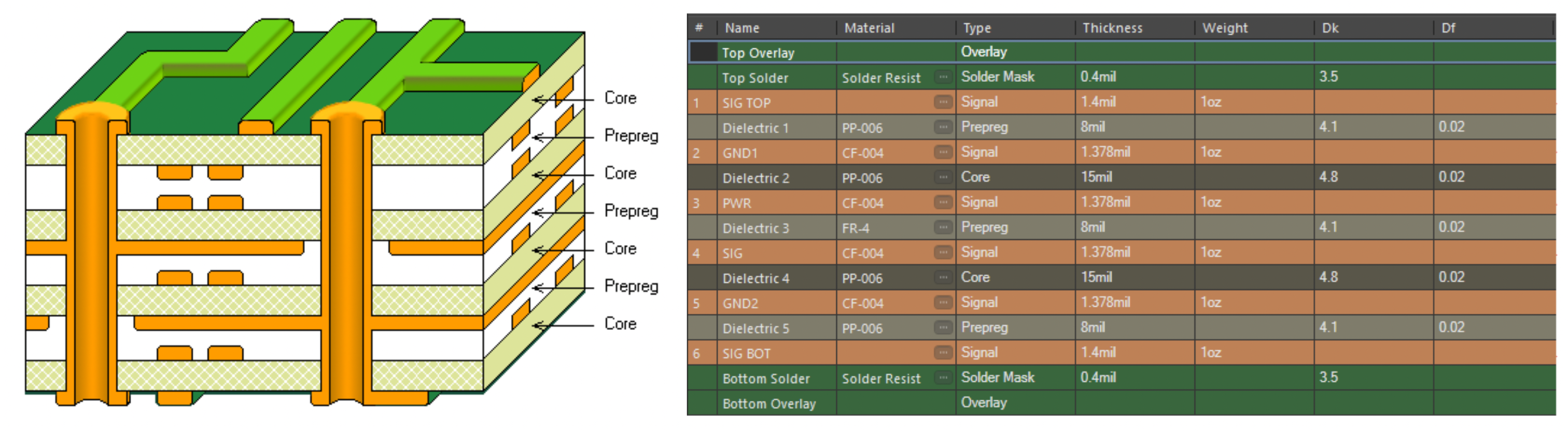
This whole affair is called a rigid PCB, because we're using a rigid, inflexible core, and it's what you'll be designing here. It's the most common type of PCB, but there's plenty of variations. You'll be designing a rigid board with two copper layers in the stackup, hence referred to as a two-layer rigid PCB or just two-layer board. The most common variation on this is a multi-layer board, where we add more layers of copper, separated by insulating fiberglass. Just for clarity, here's what the stackup would look like:
How do we make a PCB?
Making a PCB has a few steps, listed below:
- Circuit Design - where we choose the circuit that will accomplish the desired function within the provided specification.
- Schematic Capture - where we capture our circuit into a digital representation in our CAD tool.
- Board Layout
- Placement - where we choose the location of the parts on the board.
- Routing - where we actually draw the copper wires between components (called traces) and electrically connect them.
- Design Rule Checks (DRC) - where we run some automated checks on the design to look for simple mistakes - unconnected parts, short circuits and the like.
- Gerber Generation - where we make the design files required by the fab, which are called gerbers.
- Gerber Validation - where we double-check our gerbers to make sure they contain the parts they should.
- Fabrication - where we send our gerbers out to be fabricated by a fab house or fab. We'll be doing this part for ya.
We finished the circuit design and schematic capture in ex01, and now we'll run through the rest of the process. There's a lot on this list, but our design is small enough that we'll be able to get our bearings pretty quick.
Board Sizing
I know it's not on the list, but before we jump into layout we'll want to set the dimensions of the PCB we're going to make. To make things easier on the fab we're going to require all of your designs to be 1.5" x 1" - but in layout parlance we'd actually call this 1500 mils by 1000 mils (a mil is just a thousandth of an inch - it is not a millimeter). The reason for this is historical, but the consequence is that when you're working with Freedom Units™ in Altium, you're working in mils, not inches.
Go ahead and add a new PCB document in your project, and save it. Open this document, and hit the 1 key to enter Board Planning Mode. Hit Design -> Edit Board Outline, and then click and drag the edges of the board to make your board be the correct size. You can see the dimensions of your board by hitting the Properties Panel with nothing selected. Once complete, go back to 2D Layout Mode by hitting the 2 key. When editing your board shape, make it 1500 mils wide (x) by 1000 mils tall (y). In addition, keep the lower left corner of the board at the Absolute Origin (the white circle + cross).
When this is done, save the board locally.
Placement
Getting Parts on the Board
Now that our board's the right size, we'll jump into layout by putting parts on our board. But there's no parts on the board right now! Let's fix that by hitting Design -> Import Changes from Schematics. A little dialogue called an Engineering Change Order (ECO) should pop up, listing all the changes to be brought into your circuit board:
Hit Validate Changes and then Execute Changes. You should see a bunch of green checkmarks fill the ECO dialog box. Close the box, and go back to your layout.
Now, all your parts are floating off in space, and its your job to logically place them on the board. We want our parts to be arranged such that components that connect to each other should be physically close to each other. This makes our wires short, which helps with signal integrity, and our parts tightly packed, which helps us not pay the board fab for more board space than we need.
You'll do this by moving and rotating parts as you move them onto the board. The little grey wires are called airwires, and they show what components need to be connected to each other. As you move the part, they'll move with it. And once you draw the connection with a copper trace the airwire will go away.
A good way to start is to move components that are electrically close on the schematic to be physically close on the PCB. So toggle back and forth between the schematic and the PCB. Place the LED and it's current-limited resistor close to each other and to the 3.3V pin on the power connector. Place the SGP41 bypass capacitors near the SGP41 IC, and so on. Then, once parts are grouped like this, do final placement, with some tips below.
A few other things
As you're trying to figure out the optimal placement for everything, there's a few things we're going to ask you to think about:
-
Bypass Capacitors: For reasons that we've relegated to footnotes [1^], we put capacitors near the power pin on every chip. Our sensors are physically rather small, so they've only got one power pin, so we'll throw one or two bypass caps on those chips. If we had something larger (like a microcontroller) that had multiple power pins, we'd bypass each of those. But regardless of the number of bypass caps we'll need, make sure to put them close to the power pin they're bypassing.
-
Mounting Holes: Later on we'll design a 3D printed enclosure for MILO, and we'll need to make sure the board doesn't rattle around inside the case. There's a few ways of keeping your boards retained - plastic clips, 3D-printable tabs, mounting holes, hot glue...the list goes on. You'll get some choice over how you mount your board when the time comes, but as a backup we'll ask you to throw some mounting holes on your board. You can do this by adding a pad to your board (Place -> Pad), and changing its size in the properties panel once you have it selected. We'll design for a M3 screw. Be logical about the quantity and location of your mounting holes. I'm not saying that I won't be impressed if you draw a wojack on your board out of M3 mounting holes, but that's not quite what we're looking for.
-
Access to Ambient Air: While we're thinking about enclsoures, we'll need to make sure that our air sensors have, well, air to sense. And this air should be fresh too - if we were to put everything in a sealed box with no air current over the sensor, MILO would give us disappointment instead of data. Thankfully though the folks selling us these sensors have done plenty of research on how to mount them in an enclosure for best results, and so they've given us a Design-In Guide for the SGP41 and the SHTC3. Think about which side of your board the connectors should go, and on which side everything else should go.
-
Label: It's common to add a label on the silkscreen with what the board is, its version number and when you made it, along with your name and email. The reason for this is so that the end user can contact you if something goes wrong - same reason why you put your name and contact in your source code. Go ahead and add this to the top silkscreen layer by adding text to the Top Overlay layer.
-
Designators: The component designators we assigned during schematic capture are now on the board, and they're how we'll identify which part is which. But to make your boards look pretty we'll ask that all the horizontal/vertial text goes in the same direction (ie, all the vertical text is consistently ascending or descending, and similar for the horizontal font). The default font size is okay - we can go smaller but we don't really have a reason to. It'll just make board assembly more annoying for ya.
This will likely take you a while - and that's okay! When I'm doing layout I usually spend about 90% of my time on placement, and only 10% on routing. If you do your placement correctly, routing will be super straightforward!
Routing
In order to route the board, you'll draw copper traces by clicking the Interactive Routing button from the toolbar in the middle of the PCB editor, or by hitting Ctrl+W. Altium will default to 10mil traces, but if you'd like to change that, open the properties window while you're routing. If it's annoying to get to this menu because the routing cursor keeps moving the board off the screen, hit Tab to pause the routing, make your changes, and then hit Tab again to resume.
You can also add vias that route signal through the board by using your Ctrl+Shift+ rotate the middle scroll wheel (if you have one), or just placing one from the toolbar. We'll use the default via size for now, but if you want to change it you can mess with the via properties (to change just one) or the design rules (to change the default via size).
In terms of doing the wiring, we suggest to first wire up all the signals except ground. Start with the short wires, then go for the longer ones. When you correctly wire up two nodes, the airwire for that connection will disappear. Cool. All this will take a bit of time. You may find you need parts or existing wires around a bit to get more room here or there. It's an iterative process.
Then, we'll want to add a ground pour to the bottom layer of the board. This takes all the unoccupied space on the bottom of the board and fills it with copper, which is then electrically connected to ground. This is general good practice because it reduces the electrical noise on our board - we won't notice this too much since our circuity is relatively noise-resistant already, but it's standard practice and we'll do it here. And it also makes routing way easier - for the ground net at least :)
Go ahead and hit Tools -> Polygon Pours -> Polygon Manager -> New Polygon from -> Board Outline. This will add a new polygon to the polygon manager, which we'll want to connect to ground. Go ahead and change Net to GND to electrically connect it to ground, and change Layer to Bottom to have it use the bottom layer. Give it a name (we've got suggestions here), and then hit Okay. This will fill the empty space with ground pour. If you change anything on the bottom layer it won't automatically update the ground pour, so you'll need to repour it by hitting Tools -> Polygon Pours -> Repour All. Or just use the keyboard shortcut of TGA.
When you repour ground pour will automatically reroute itself around any traces you have on the bottom of the board, but thanks to Spooky Magic the ground pour will work better with large, unbroken regions of copper. Try to keep as much of your routing on the top layer as you can so you don't slice up your ground pour with traces on the bottom. Don't get too worked up about this, but avoid it if you can.
Now, with the ground pour done, you can wire up all your grounds, but starting a wire from a ground pad, then adding a via to the ground pour side. So the grounds will end up looking like little wire stubs + vias. Nice and sweet.
Design Rule Check (DRC)
Once you think you think you're finished routing your board, it's time for DRC. This is Altium's set of automated checks, which we can run by hitting Tools -> Design Rule Check -> Run. It's default settings can sometimes be a little conservative, so in addition to catching things that'll definitely break your design (traces you forgot to route, or traces that overlap and short out) it'll also catch things that might break your design. We'll leave it to your intuition to figure out which are which, but ask if you'd like us to have a look! We'll check your work at the end anyway.
Gerber Generation
Once you're passing DRC (or more realistically, failing it acceptably), we'll want to generate Gerbers. These are files that describe what each layer looks like on your board, so there’ll be one to show where the copper goes, one for the silkscreen, another for the soldermask, and so on. Here are the Gerbers for our sensor board's top and bottom copper:
And if you’ll notice, there’s a bunch more for the other layers. We’ll need to get Altium to generate these so we can give them to the fab, along with some extra information about how we’d like our boards to be made.
Altium generates Gerbers with something called an OutJob - a little tool that can make any kind of outputs we'd want from our project, including Gerbers. Here we'll just be using it for that, but you can also have it generate .pdfs of your schematics, a .csv or .xlsx of your BOM, or a .step of your PCB geometry. We've got a preconfigured OutJob for 2-layer boards that we stole from FSAE seems to work well. It's here. If you need to make a custom one, the Altium Docs have got you covered.
It's worth noting that our Gerbers only include what goes on each layer - but some of the features on our boards go through layers! Vias, through hole pads, and mounting holes all get drilled into our board, and the gerbers don't specify those locations. So we'll also need a list of holes to drill, which is commonly produced as a .txt file with the X/Y coordinates of each hole, along with the drill size. This is called the NC Drill file, because we were making PCBs back when CNC machines were just NC machines.
Go ahead and add the OutJob to your project by dragging it on top of the project in the Project window, or by right-clicking the project and hitting Add Existing to Project and selecting the OutJob. Double click the OutJob, hit generate, and you should be off!
If you add the OutJob to your version control in the side panel (right click the OutJob, hit Version Control, and then Add to Version Control) then A365 will be able to use it in the web portal. This means that you'll be able to click the download button in the corner of your Project page and download your Gerbers as a .zip, schematic printouts as a .pdf, or CAD as a .step. This is incredibly handy.
Gerber Validation
We'll want to make sure our gerbers look good before we send them off to the fab. Open the gerber file for each layer, and make sure they look like what you'd expect. For instance, the top copper should have just traces, pads, and vias on it - but the bottom copper should have the pour, and maybe a trace or two. Again, let us know if you've got questions.
Saving your Work
Save your work to A365 using the same method as last time. You should be able to go to your folder on the A365 workspace and see your board under your project's PCB tab. If you can't see it there, then neither can we. Click the box below once your work is done and in A365. Don't edit your work after you've turned it in.

[^1]: The traces on your board act as antennas that unintentionally radiate the signal they're carrying out of the trace, into other traces and the environment. Take a bunch of traces on a board transmitting into and out of each other all the time, and you get a bunch of noise. We don't want this noise getting into the power rails of our chip, because power gets routed to pretty much everything inside the chip, so any noise in power is seen in pretty much the entire chip's outputs. Which is bad. And there's another reasons why we'd want bypass capactiors, but I'm out of space in this footnote.