MILO sensor board schematic capture
Please Log In for full access to the web site.
Note that this link will take you to an external site (https://shimmer.mit.edu) to authenticate, and then you will be redirected back to this page.
What is MILO?
MILO is our air quality monitor that we'll create in the first part of the term. We'll introduce MILO in detail in Lecture 03. But we don't need to wait for that to get started. Head over to the MILO project page and poke around. MILO's hardware is loosely divided into three subsystems: sensing, computation/communication, and power management. We've physically partitioned these three subsystems into three printed-circuit boards (PCBs).
In this lab we'll start the design for the simplest one - the sensor board.
Learning Objectives
In this exercise, you'll create the schematic for the MILO's sensor board in an electrical design tool called Altium. It'll let us capture our design as a schematic, which we'll later turn into a printed circuit board (PCB) through a process called layout. Here, you'll do a little circuit design, and hunt for information in datasheets.
You'll need a working copy of Altium for this lab. The instructions for getting it are here, along with the rest of the course software.
Circuit Schematics
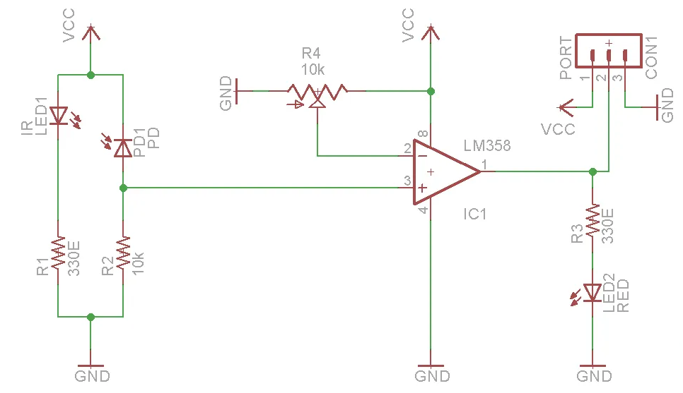
The first step of designing a PCB is drawing a schematic, which depicts all of the components and how they are connected. This process is called schematic capture. Schematics are how electrical engineers represent circuits logically, and let us do circuit design without having to think about where exactly the physical components will live in real life. They look something like this:
Altium has it's own set of tools that'll help us make sure that the circuit our schematic represents actually works. Schematics are also used by circuit simulators like LTSpice that toss in physical models of each component, and simulate the circuit through time. If you do it right, this helps verify that the circuit will perform as expected.
If you haven't used Altium before or if you want a refresher, we recommend the following Altium tutorials on schematic capture:
-
Altium Tutorial from 6.S092, read up until the "Layout Basics" section for this week.
Specifications & Design
The design specs for MILO are listed on it's page, and it'll need to sense temperature, relative humidity, and air quality (VOC/NOx). We've chosen to use the following two sensors, and their datasheets are linked:
The SGP41 and SHTC3 communicate with a microcontroller via I2C, and both run off 3.3V, so our sensor board will include connectors for power (3.3V and GND) and I2C communications (SDA and SCL lines). All this is specified in the datasheet.
What else do we need to specify?
In designing this subsystem, like many others in this class, we need to think through the interactions with other subsystems, as well as test and verification (and thus debugging!). For this first design, we'll basically tell you what you need to include and why. For future designs, you're more on your own!
-
Physical layout: sometimes we can put stuff wherever we want on a board, sometimes we can't. This is an example of the latter. The manufacturer has a detailed guide about arranging the SGP41 in particular. For example, both these sensors need to be exposed to the environment they want to measure. They also both should be removed from parasitic heat sources, or materials that will off-gas. This doesn't affect the schematic design, but it will affect PCB layout. More importantly, we'll see next week that it is advantageous for the sensors to be on one side of the board, and the connectors on the other. Stay tuned for that!
-
Connectors: how are we going to get the electrical signals from this board onto the others? We'll need cables to do this - but there's an incredibly large selection of wires and connectors to build our cables from. Here we'll use a 2-wire JST connectors, and then some generic 22-gauge wire between them. Why? Easy, common, and we don't have any crazy specs in terms of voltage or current.
-
Debugging: We all hope our HW/SW works the first time - but it won't! So you need to make debugging easier. On the hardware side, that means:
- Making sure all important pins on the chips are "brought out" so they can be probed, or soldered to, and
- Including what are known as test points on key signal paths. Test points allow us to probe the circuit to verify it is working correctly. For this board, think about what signals would be useful to be able to test if the board does not work right away.
- Including status LEDs. It's annoying if you have to hook your system up to an oscilloscope or computer to know if it's on, or working. So we add status LEDs that help us know at-a-glance what's going on.
-
Testing & verification: related to debugging is testing. How do we know if our sensors work? We need to set up tests, same as the "unit tests" in software engineering. For an environmental sensor, that means testing across T, RH, VOC/NOx levels. Not easy! We'll return to this later.
Schematic Design on Paper
Before drawing the schematic in Altium, we will first sketch things out on paper.
IC manufacturers will often provide reference or typical application designs in the datasheets. These show an example design that covers most of the use cases of their specific part - they do this to make your job as a designer easy, so you'll use their parts! For now, we're going to follow their lead, and use their reference designs for our two sensors. We'll find those in:
-
Check out Figure 6 on page 8 of the SGP41 datasheet. The diagram shows how the sensor should be connected for correct operation. Notice that it has two pins SDA and SCL for talking to a microcontroller over I2C (quick refresher on how I2C works).
-
Also take a gander at Figure 6 on page 6 of the SHTC3 datasheet. It too has a diagram for how the sensor should be connected. It also has SDA and SCL pins for I2C communication.
We'll be putting both of these designs on the same PCB - but the reference designs don't know that! It's your job to combine the two into a single circuit. Go ahead and sketch this out on paper - you'll need more than just the two ICs.
-
You'll be able to share ground and power wires across the two sensors.
-
You'll also be able to share the R_p pull-up resistors across the two ICs. On a single design, only one set of resistors is needed for the SDA and SCL lines.
-
Next, mark the wires you think will need test points. A simple rule of thumb for us: put test points on each separate signal, aka power, ground, SDL, SCA.
-
Next, we need to add in status LEDs. We recommend a status LED on the 3.3V power line. If you'd like to add others, feel free. Each LED will need a series resistor connected between the LED's anode and the signal being measured (in this case, 3.3V). This so-called current-limiting resistor (details here, or here) needs to be of the right value so that the right amount of current goes through the LED: too much current and the LED will burn out, and it will consume too much power; too little current and the LED will not turn on or will be really dim. The amount of current depends on the LED. You have a choice of four colors, all from the same part family:
- Red: HSMS-C170
- Yellow: HSMY-C170
- Green: HSMG-C170
- Orange: HSMD-C170
The datasheet provides the typical (forward) voltage to achieve the 20 mA they use as their standard brightness (see Table 5). Pick your color, and calculate your resistance given our 3.3V supply voltage. There's also a nice discussion of resistor sizing in the 6.S092 Altium Tutorial.
We don't ask you to hand in the paper schematic, but you'll need it to keep yourself from getting confused as you're putting things into Altium. We're teaching you both design intuition and a new tool here, and your paper schematic is the bridge between the two - it's your map and anchor. Put some care into it. Once it's complete, let's capture it in Altium.
Schematic Capture
Fire up Altium, go to our Altium workspace, and make yourself a folder, and name it with your kerb. This will be your folder for the course, and go ahead and make a new design inside called {your_kerb}_sensor.
Placing Components
The first step is placing all the components our circuit needs into the schematic.
Let's add our passive components (resistors, capacitors, LEDs) first. To reduce the size of our boards, we'll be using surface mount (SMD) components when possible. SMD components are mounted directly to the face of the board rather than requiring a through-hole. Surface mount parts come in a range of standard packages and sizes. For our resistors, capacitors, and LEDs we're going to standardize things by always using 0805 parts. 0805 refers to the dimensions of the package, in this case 0.08" by 0.05" (or, 2 mm by 1.2 mm, for those in more modern societies). This choice is a bit arbitrary, but 0805 parts are common, small enough to create compact boards, and large enough to put together by hand.
Part of this abundance of choice means that we'll have a little nuance when putting our components into the schematic. Altium has two sources for components:
- Manufacturer Part Search (MPS) - which is a big CAD library that's built and mantained by the company. When we pull parts from MPS, we pull a specific part. If we were to search for a 10K 0805 resistor, we'd get thousands of results, and choosing one is really darn annoying. But if we were to search for a very specific part - like our SHTC3 - we'd get exactly one result, which CAD from the manufacturer to match. Which is super handy.
- Workspace library - which is our own, class-specific CAD library that's built and maintained by us.
Where we want to pull parts from depends on what the part is. For super generic parts like resistors, capacitors, and LEDs: we've added some generic versions to our workspace library to prevent you from the unfortunate situation mentioned above. We've also added some other parts to the workspace libraries - parts we had to manually add or tweak the CAD on.
All this means that as a general principle, you should check for the part in our workspace library first, and if they're not there, hunt for it in MPS. We'll show you how to do that below.
Workspace Libraries
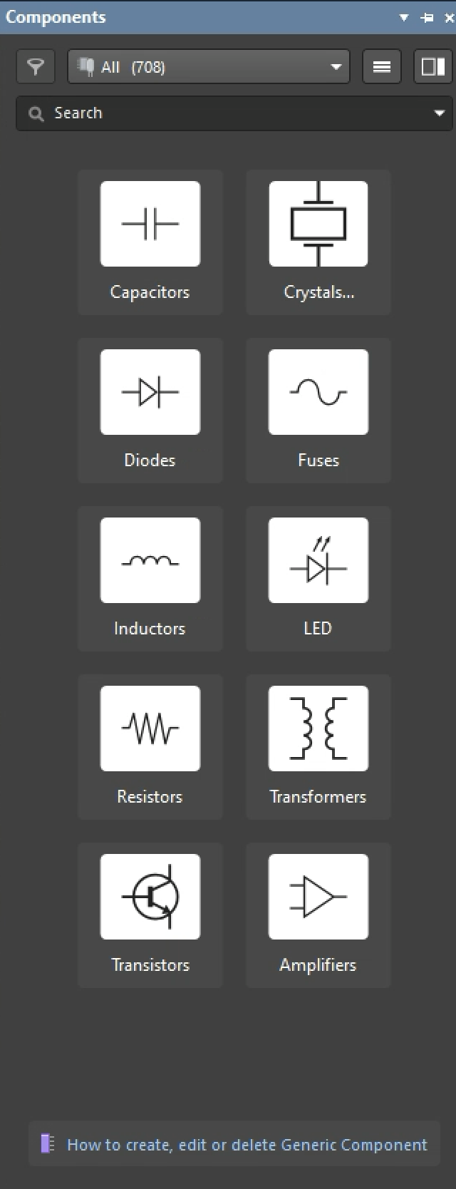
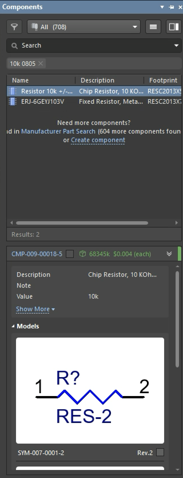
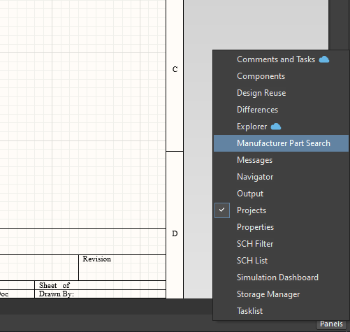
Let's walk through placing a 10K 0805 resistor, which we'll grab from our workspace library. Click Panels in the bottom right corner, then Components. If it gives you a blue button that says Use Existing Components, click it - no worries if not though. You should see something that looks like this:
Go ahead and find the part you want with the search box, and then either drag it onto the schematic, or right click and hit Place.
Do this for the remaining resistors and capacitors. Now, if the value you want isn't listed, do two things:
- Right-click on the resistor, select Properties, and then update the Comment (you can change the description if you want as well).
- Next, in the same Properties side menu, under "Parameters", click "All", and "Value" should show up. Change it to whatever you want -- the text next to the resistor in schematic should also change.
Other parts to insert from our Workspace Library:
- SGP41 Gas Sensor -- use the one in our workspace library because we've adjusted it a bit
- B2B-XH-A(LF)(SN) JST connector (2 of them)
- Test points: search for "testpoint" and choose the 5003 part, which is a thru-hole test point (4 of them)
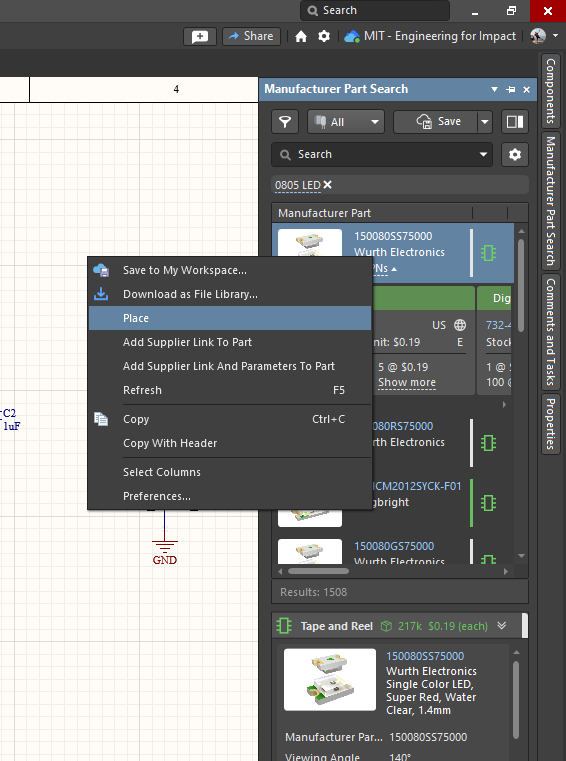
Manufacturer Part Search (MPS)
Let's next walk through placing the SHTC3 as an example - it's not in our Workspace libaries, and we'll be using the manufacturer CAD for it. Click the Panels button in the bottom right corner of the screen. This brings up a search window that allows you to search for parts from a number of manufacturers.
Here you can see how many of each component are in stock and how much they cost. If we search for SHTC3, the top result is the Sensirion part. That's the one we want. Clicking on a part in the search window brings you to a webpage with more information on the part specifications.
When you want to place the part, just right click it, and hit "Place".
You'll also need to use MPS for the LED. In this case, search for "HSMS-C170" and select the Broadcom Avago part. Do this no matter which color LED you brought in. Why don't we care? Because all we really care about here is the symbol and the footprint, which are identical across all 4 LED colors.
Assigning Designators
Electrical engineers use something called a Designator to keep track of parts in the circuit. A designator is basically a unique ID for the component that describes what part it is. For instance, a designator of R42 would describe the 42nd resistor on the board, and C89 would represent the 89th capacitor on the board. The utility of this will be made very apparent when we go to layout our boards next week.
For now though, we'll need to assign designators to each component. We'll have Altium do this automatically since we don't care what the number in each designator is. Go ahead and hit Tools, Annotation, and Annotate Schematics Quietly. You should see all the R?, C?, and U? on your schematic get replaced with real designators.
While you're at it, edit the "Comment" for each part so it is useful: 10k, 1u, etc. That will make your schematic easier to read.
Connecting Components
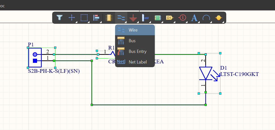
At this point, your schematic should contain a bunch of randomly arranged, unconnected parts. Click the wire tool in the toolbar in the top center of your editor, and wire the parts together. This connects them electrically.
You'll also want to arrange your parts so that you don't end up with a ratsnest once everything's connected. You can rotate your parts by hitting spacebar with the part selected, and you can mirror the part with the X and Y keys - which one you press determines the axis it's mirrored on.
As you start to draw more than a few wires, eventually your wires will cross and eventually your design will get messy. See the next section below about how to make the design neater via use of Nets. In particular, you may find it useful to Power and Ground ports in your design, which are again accessible from the top bar.
Nets / Net Labels
Thus far we haven't had a ton of connections between components, and there haven't been that many components to connect to. That goes away for larger designs, which will turn into a ratsnest of chaos if we only connect things with wires. We'll need some notation to help us keep our schematics tidy and legible. The electrical engineers of yore decided that the best way to do this was by putting a label next to the wire to label the signal - and when we want to use this signal elsewhere, we just put the same label next to that wire, making them electrically connected. This means that everything with the same name is electrically connected. Straightforward enough.
Altium (along with most electrical design tools) implements this feature as something called a net, which is just that named wire. We assign wires to nets by throwing a net label on the wire, and any two wires that have the same net label attached to them will be electrically connected. For this to work, the names must match exactly, but we get to pick the names. And as long as we name our nets things that make sense, we can make our schematic make sense to whoever's reading it. Just like variables in code.
Here's an example:
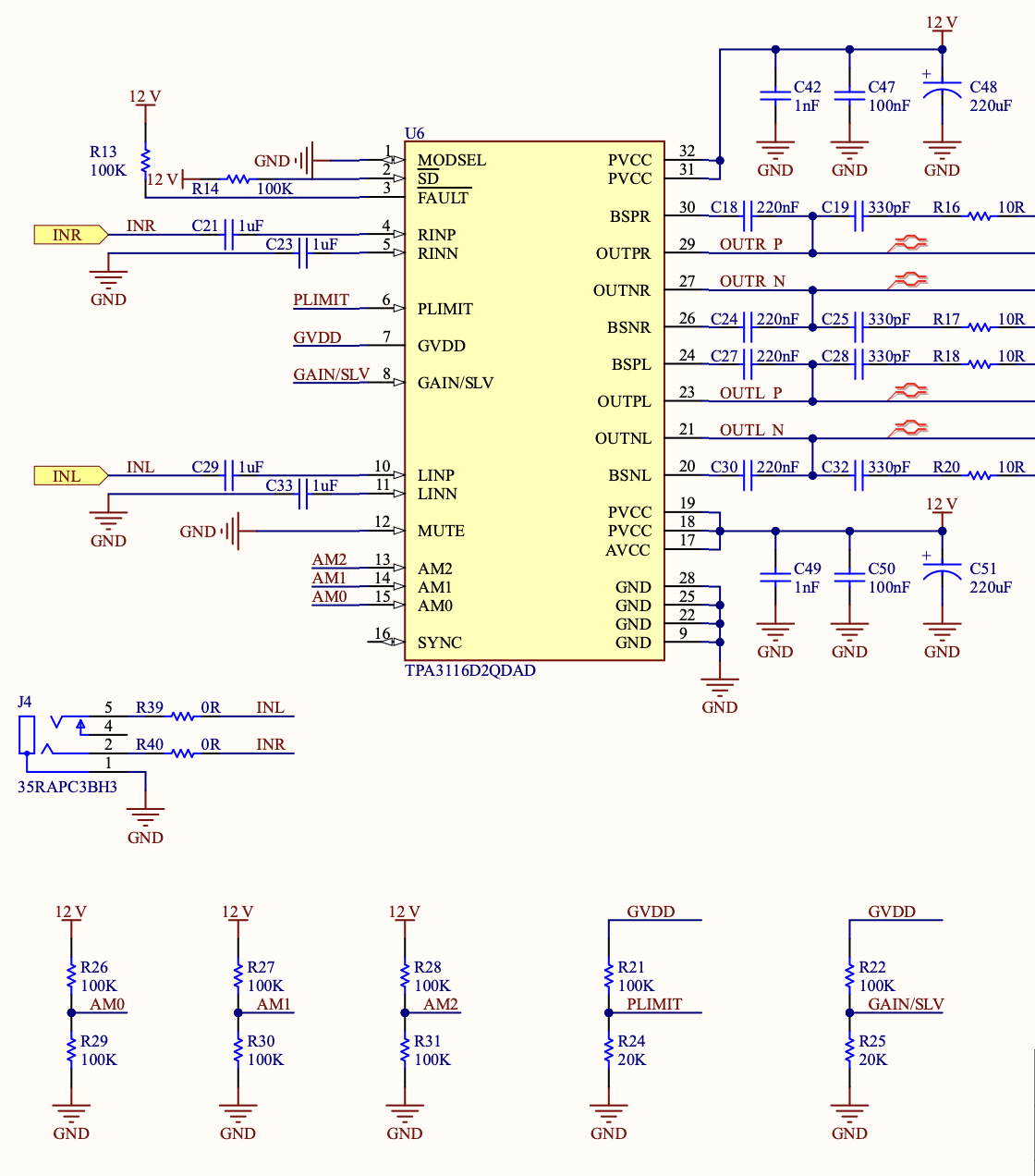
If you notice, we're using net labels for signals like INR, INL, PLIMIT, GVDD, and so on. See if you can find where else these map to on the schematic sheet!
Final Schematic Requirements
Before moving on, your schematic should meet the following requirements. Your schematic should have:
- One B2B-XH-A(LF)(SN) JST connector where the pins are SDA and SCL to provide access to the I2C interface.
- One B2B-XH-A(LF)(SN) JST connector to provide 3.3V and GND.
- A LED (in an 0805 package) indicating when the board is connected to power.
- Test points on SDL, SCL, 3.3V, and ground and SCL nets for debugging. The test points can be placed anywhere on those nets.
- Appropriately named nets for SDA, SCL, GND, and 3.3V (or VDD).
- The SGP41 and SHTC3 should be wired to 3.3V, GND, SDA, and SCL according to their component datasheets.
- Very likely 4 resistors and 3 capacitors.
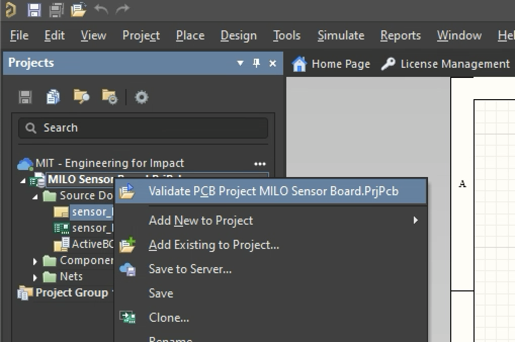
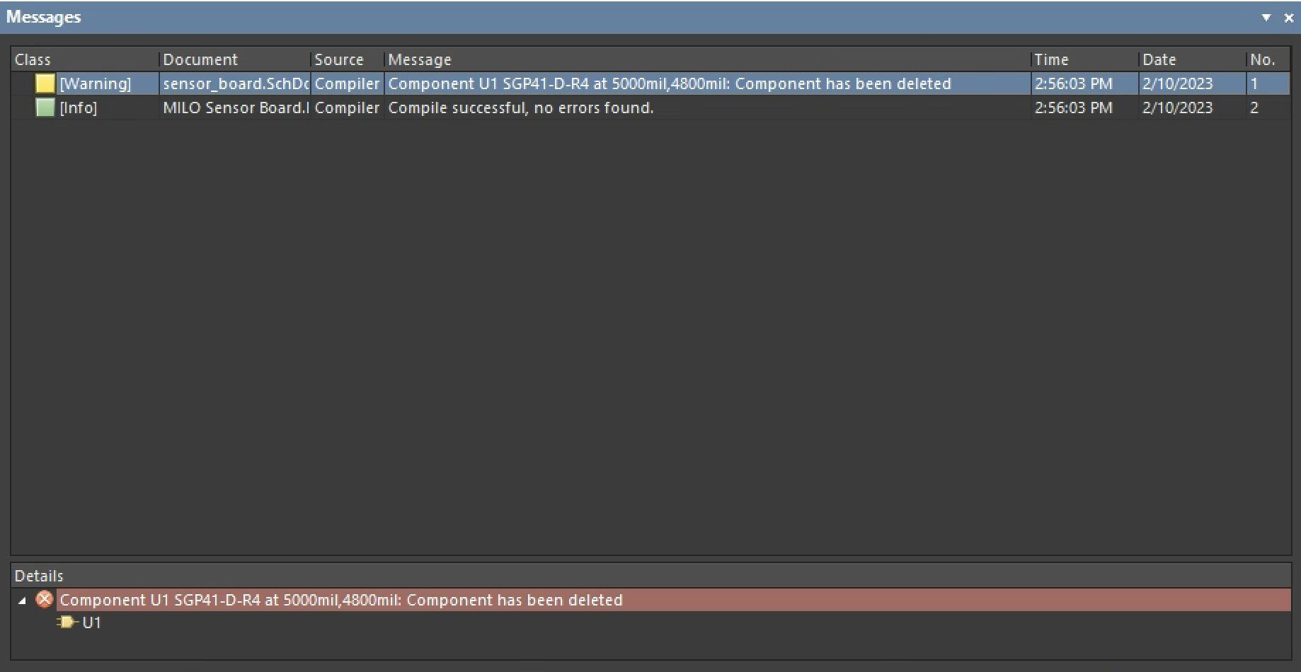
Your schematic should pass Altium's Electrical Rule Check (ERC), which is a set of automated checks it does to make sure your design looks okay. You can run it by right clicking your PCB project in Altium, and hitting Validate, like so:
If you've got errors, you'll see a Messages window pop up with a list of what's wrong. If you don't have any errors no window will pop up, but you can see any warnings by opening the Messages window manually. Go to Panels and click Messages to do this, and you'll see something like this:
Once you are satisfied with your schematic, save it to A365, which you can do by clicking Save to Server and entering a commit message:
Click the button below once it's saved so we know you're finished. You can submit multiple times, we'll use the last submission time.

What's next
In Lab02 we'll do schematic reviews. You'll show us and your team your schematic, and everyone will provide feedback (same as at a code review). We'll then turn our schematic into an actual PCB in EX02 when we layout the board.