MILO MCU and power board schematic capture
Please Log In for full access to the web site.
Note that this link will take you to an external site (https://shimmer.mit.edu) to authenticate, and then you will be redirected back to this page.
Desiging the MILO system other boards
Learning Objectives
With your first schematic drawn and reviewed, it's now time to perform schematic capture for the rest of the MILO hardware node (aka the box).
From our MILO system diagram, we can see that the hardware is broken into three boards.
Divide and conquer
We're going to divide the team into two sub-teams: one team will do the power management board, the other will do the MCU board. So your first task is to agree as a team who will do what.
To help you decide how to divide, let's talk a bit about what goes into each subsystem.
MCU subsystem
The MCU subsystem is the brains of the MILO hardware node. We need a central controller to interact with the sensors and to relay that information to the server. That is the MCU subsystem.
We're going to make life a bit easier, but using a fairly powerful MCU: the ESP32-C3. Even better, we can purchase the ESP32-C3 in a module that includes the WiFi antenna. Better still, the module itself has been FCC certified, so it meets our regulatory spec straight-away.
There are actually several ESP32-C3 modules we can purchase:
The main difference is that the MINI has a smaller footprint than the WROOM. But the footprint of the WROOM is amenable to hand-soldering. So we'll go with that, since eventually we'll have to assemble the boards by hand.
Even once we've picked the WROOM there are multiple sub-variations (yes, this stuff gets detailed!). Go to the datasheet and figure out how many variations there are.

To make our lives easier, we want the one with an integrated antenna, and we don't need a wide temperature range, given our operating temperature spec.
OK, so we have a part, so what else do we need for our schematic? Well, we'll want all the things we had for our sensor board:
- Connectors for power and data
- Status LEDs
Reset Button
In addition we probably need a way to reset the MCU without having to plug/un-plug. So it's good to have a button for that.
Section 3.2 of the ESP32-C3-WROOM-02 datasheet lists the function of each pin on the module. We can see the EN pin (pin 2) resets the MCU when it is pulled low. It also says not to leave the pin floating, so we'll need a pull-up resistor between this pin and the 3.3V line to make it default to high. As a rule of thumb, we'll use 10k ohm resistors for our pull-up resistors. We'll also add a button between this pin and ground so that when we press the button, the pin gets pulled strongly to ground resetting the MCU.
Draw out this button and pull-up resistor on your paper schematic.
Boot Sequence and Strapping Pins
Another thing we need to consider is that the MCU needs to be put into a certain state in order to be ready to receive new firmware. This can sometimes be done via software (that's why you can often "flash" new code onto your MCU just via software control), but it's good to have a physical button in case things go awry.
Check out section 3.3 of the ESP32-C3-WROOM-02 datasheet. Here it describes how the ESP32 can be booted into SPI Mode or Download Mode. In SPI mode, it executes any uploaded code as expected. In Download Mode, code may be "flashed" to the MCU.
We can control which mode the ESP32 boots into by adding pull-up or pull-down resistors to several "strapping pins" defined in section 3.3 of the datasheet and using a button to pull the voltage the other way when it is pressed. We want our system to default to the SPI boot, but we'd like to maintain the option to put it into Download mode via a button press if we need to.
In your paper schematic, add pull-up resistors between the necessary pin(s) and the 3.3V line.
In the above concept question, we identified a pin that boots the MCU into SPI Mode if it is high and Download Mode if it is low. We'll use a combination of a pull-up resistor and a button to pull the pin high when the button is not pressed, and low when the button is pressed. Add this button to your paper schematic tying the pin to GND when the button is pressed.
Beyond that, the MCU schematic will need typical components: some decoupling capacitors, pull-up resistors, and the such.
We're not going to explicitly tell you everything that should be on this board. But you can look at reference designs, such as on the datasheet, or other similar boards, like the Seeed Studio XIAO ESP32C3](https://www.seeedstudio.com/Seeed-XIAO-ESP32C3-p-5431.html), and so on.
Power management subsystem
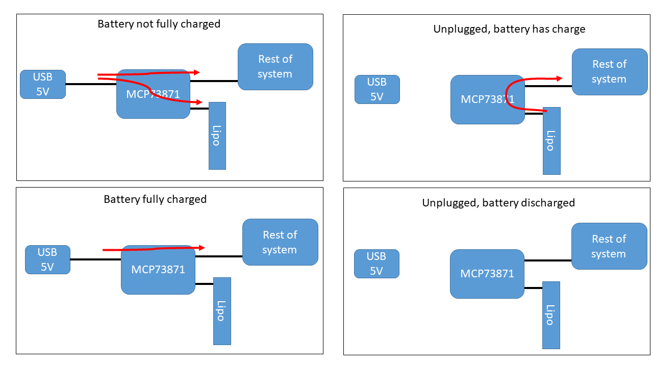
The power management subsystem has one primary goal: deliver power to the rest of the system. But when we drill down, it gets a bit complicated.
In order to be portable, we decided to power MILO via a LiPo battery. A single-cell LiPo battery has a nominal voltage of 3.7V (a bit more when fully charged, and decreasing as it discharges). We want to take that voltage and convert it to the 3.3V that the rest of the system needs. In some cases it's not absolutely necessary to do so -- this voltage conversion (with a voltage regulator) takes extra parts and space and thus cost. However, we want to avoid downstream issues that can arise from a varying supplying voltage, so we'll incorporate a 3.3V regulator.
But eventually the battery will discharge, so we need a way of charging it back up. So we need some sort of integrated circuit to charge the battery. LiPo batteries can be dangerous, so specialized ICs are used to make sure the batteries charge at the right rate and to the right voltage.
But it gets even more complicated. If we're running off of the battery, and the battery gets too discharged, we'd like to be able to plug the system in, and have the system continue working, while the battery is charging. After all, when you plug your phone in to charge, you expect the phone's battery to charge and the phone to still work.
So really what we need is some magical IC (or ICs) to manage the power, directing power to/from the battery, to the system, from the wall, and so on. Sounds complicated.
Luckily, it's complicated but extremely commonly needed, and hence companies have created solutions to do this. These systems go under various interrelated name: battery management system (BMS), power management IC (PMIC), battery chargers, and so on.
We'll be using the MCP73871. This remarkable little chip (~$2!), includes "load sharing" (aka automatically directing power to the system or the battery), and battery charge management (charge the battery).
Basically, the system operates in a few different modes:
Power board functions
Now, we're mostly done, but the MCP73871 will be more than happy to send 5V to the rest of the system when under USB power, and the raw battery voltage when under battery power. So we will need to insert a regulator at the output of the MCP738731.
The regulator's job is to take whatever voltage comes in and output 3.3V, with the important caveat that the voltage coming in is >3.3V. There are basically two ways to do this: we could basically burn away the extra power and output 3.3V, or we could somehow transform the input voltage into 3.3V without losing (much) power. The first way is a linear regulator, the second uses a switching regulator. If we really cared about power efficiency, or we wanted to make a smaller voltage into a larger voltage, we could use a switching regulator. In our case, we think we'll have plenty of power for MILO, and the linear regulators are inexpensive, small, and require very few external components.
So we'll use a linear regulator. To pick one, we need to know the range of input voltages, the desired output voltage, the current that we need to supply, and of course cost constraints, size constraints. We have chosen the AP7361C-33Y5-13. This is one part i nthe AP7361C family. The "33" means it outputs 3.3V. The "Y5" indicates that the package is an SOT89-5 (pretty easy to hand solder). It's inexpensive (~$0.50 at our quantitites), and readily in stock.
So now we can get a handle on what goes into this board:
- MCP73871, AP7361C-33Y5-13
- Some connectors (enough to power the other boards in the system)
- Some status LEDs, and other external components (resistors, caps)
This board uses two nontrivial ICs with datasheets we'll have to reference for the schematic design. The MCP73871 in particular has a lot going on, so we'll break down some of the datasheet here.
Reference Circuit and Pin Descriptions
First, take a look at page 2 of the datasheet. It has a typical application circuit giving a reference design for many of the details of the schematic.
Section 3.0 starting on page 17 has a table of pin functions as well as written explanations of which pin does.
VPCC and TE For our simple MILO system, there are a couple features of this chip we'll ignore: the voltage proportional charge control (VPCC pin, section 3.3) and the internal safety timer (TE pin, section 3.14). Read those sections of the datasheet to determine how to properly deactivate them.
SEL Pin The SEL pin (pin 3) determines the maximum output current that the MCP73871 will supply to the system and the battery charger when the board is plugged in to a power source. We'll be powering this board from a micro-USB connector, so we want this maximum current to reflect the USB specificiation.
CE Pin The CE pin (pin 17) is the "charge enable" pin. When this is high, the IC allows battery charging.
Status Pins
The MCP73871 has three output status pins that switch between a high-impedance output and a low voltage depending on the internal state of the IC. Table 5-1 on page 25 has a handy reference for what pin states correspond to the various internal states.
For our MILO board, we want to be able to easy tell the state of these pins for easy debugging. In your paper schematic, add status LEDs to each of these pins.
Thermistor
According to section 3.15, the MCP73871 expects a 10k negative temperature coefficient (NTC) thermistor to run between pin 5 and GND.
Many LiPo batteries have this thermistor built in and the MCP73871 uses it to monitor battery temperature and stop charging if the battery gets too hot. Our batteries don't have this built in thermistor, so we can add a normal resistor to emulate this.
Programming Pins
The MCP73871 has three "programming" pins that adjust different parameters of the battery charging cycle, these pins are creatively named PROG1, PROG2, and PROG3.
Check out this article if you'd like to learn more about LiPo battery charging. The short version is that the MCP73871 will go through a fast charging cycle which applies a relatively high constant charge current and then switches to a constant charge voltage mode.
In this IC, PROG1 is used to set the fast charge current. PROG3 is used to set the "charge complete" current. When the charger is in constant voltage mode, the charging current will decrease as the battery voltage approaches the charging voltage. When this charging current falls below a threshold set by PROG3, the IC will halt battery charging.
When charging from a USB interface, PROG2 sets the maximum current the IC will pull from the USB source. For our MILO boards, go with the higher current draw.
It can be tricky to parse through the datasheet, so we'll highlight some important sections here:
- Section 3.8: more details about PROG1
- Section 3.9: more details about PROG2
- Section 4.3
- Section 4.5 and Equation 4-1: how to choose a value for PROG1
- Section 4.7 and Equation 4-2: how to choose a value for PROG3
For our MILO system, choose PROG1 such that the fast charge current is 1A and choose PROG3 such that the completion current is 100mA.
Linear Regulator
The MCP73871 directly outputs whatever the source voltage is, so if our battery is currently supplying 3.7V, that's what we'll get out of the OUT pin of the MCP73871. The rest of our boards expect a 3.3V supply and this higher voltage might damage them. One solution to this is to add a linear regulator to our board. As mentioned above, we'll be using the AP7361C-33Y5-13.
This part is quite a bit simpler, take a look at page 11 of the data sheet for an example circuit.
Add this IC into your paper schematic so that it regulates the output of the MCP73871 down to 3.3V.
Draw your schematic
Now that you've seen what's involved in each of these two subsystems, pick which team members will design which boards. Remember, half should do the MCU board, half the power board.
Then, each sub-team should develop paper schematics by studying the typical application diagrams for their systems. You can talk among subteams, and between subteams, but ultimately each person should have their own design.
Next, start up a new project in Altium and draw your schematic.
Submitting your design
Once you are satisfied with your schematic, click the button below so we know you're finished. You can submit multiple times, we'll use the last submission time.
What's next
In Lab03 we'll do schematic reviews of these two boards.
Laying Out the Board
We'll lay out the boards in EX03.